Cypress CY7C1302DV25 User Manual
Page 2
CY7C1302DV25
Document #: 38-05625 Rev. *A
Page 2 of 18
Selection Guide
CY7C1302DV25-167
Unit
Maximum Operating Frequency
167
MHz
Maximum Operating Current
500
mA
Pin Configuration
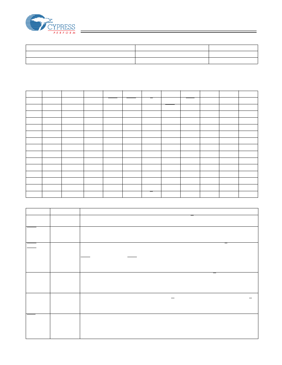
165-ball FBGA (13 x 15 x 1.4 mm) Pinout
CY7C1302DV25 (512K x 18)
1
2
3
4
5
6
7
8
9
10
11
A
NC
Gnd/144M NC/36M
WPS
BWS
1
K
NC
RPS
NC/18M Gnd/72M
NC
B
NC
Q9
D9
A
NC
K
BWS
0
A
NC
NC
Q8
C
NC
NC
D10
VSS
A
A
A
VSS
NC
Q7
D8
D
NC
D11
Q10
VSS
VSS
VSS
VSS
VSS
NC
NC
D7
E
NC
NC
Q11
VDDQ
VSS
VSS
VSS
VDDQ
NC
D6
Q6
F
NC
Q12
D12
VDDQ
VDD
VSS
VDD
VDDQ
NC
NC
Q5
G
NC
D13
Q13
VDDQ
VDD
VSS
VDD
VDDQ
NC
NC
D5
H
NC
VREF
VDDQ
VDDQ
VDD
VSS
VDD
VDDQ
VDDQ
VREF
ZQ
J
NC
NC
D14
VDDQ
VDD
VSS
VDD
VDDQ
NC
Q4
D4
K
NC
NC
Q14
VDDQ
VDD
VSS
VDD
VDDQ
NC
D3
Q3
L
NC
Q15
D15
VDDQ
VSS
VSS
VSS
VDDQ
NC
NC
Q2
M
NC
NC
D16
VSS
VSS
VSS
VSS
VSS
NC
Q1
D2
N
NC
D17
Q16
VSS
A
A
A
VSS
NC
NC
D1
P
NC
NC
Q17
A
A
C
A
A
NC
D0
Q0
R
TDO
TCK
A
A
A
C
A
A
A
TMS
TDI
Pin Definitions
Name
I/O
Description
D
[17:0]
Input-
Synchronous
Data input signals, sampled on the rising edge of K and K clocks during valid Write opera-
tions.
WPS
Input-
Synchronous
Write Port Select, active LOW. Sampled on the rising edge of the K clock. When asserted active,
a Write operation is initiated. Deasserting will deselect the Write port. Deselecting the Write port
will cause D
[17:0]
to be ignored.
BWS
0
,
BWS
1
Input-
Synchronous
Byte Write Select 0, 1, active LOW. Sampled on the rising edge of the K and K clocks during
Write operations. Used to select which byte is written into the device during the current portion of
the Write operations. Bytes not written remain unaltered.
BWS
0
controls D
[8:0]
and BWS
1
controls D
[17:9].
All the Byte Write Selects are sampled on the same edge as the data. Deselecting a Byte Write
Select will cause the corresponding byte of data to be ignored and not written into the device.
A
Input-
Synchronous
Address Inputs. Sampled on the rising edge of the K (read address) and K (write address) clocks
for active Read and Write operations. These address inputs are multiplexed for both Read and
Write operations. Internally, the device is organized as 512K x 18 (2 arrays each of 256K x 18).
These inputs are ignored when the appropriate port is deselected.
Q
[17:0]
Outputs-
Synchronous
Data Output signals. These pins drive out the requested data during a Read operation. Valid data
is driven out on the rising edge of both the C and C clocks during Read operations or K and K
when in single clock mode. When the Read port is deselected, Q
[17:0]
are automatically
three-stated.
RPS
Input-
Synchronous
Read Port Select, active LOW. Sampled on the rising edge of positive input clock (K). When
active, a Read operation is initiated. Deasserting will cause the Read port to be deselected. When
deselected, the pending access is allowed to complete and the output drivers are automatically
three-stated following the next rising edge of the C clock. Each read access consists of a burst of
two sequential transfers.