Thermal resistance, Capacitance – Cypress CY7C1302DV25 User Manual
Page 14
CY7C1302DV25
Document #: 38-05625 Rev. *A
Page 14 of 18
Thermal Resistance
[20]
Parameter
Description
Test Conditions
165 FBGA Package Unit
Θ
JA
Thermal Resistance (Junction to Ambient)
Test conditions follow standard test
methods and procedures for measuring
thermal impedance, per EIA/JESD51.
16.7
°C/W
Θ
JC
Thermal Resistance (Junction to Case)
2.5
°C/W
Capacitance
[20]
Parameter
Description
Test Conditions
Max.
Unit
C
IN
Input
Capacitance
T
A
= 25°C, f = 1 MHz,
V
DD
= 2.5V.
V
DDQ
= 1.5V
5
pF
C
CLK
Clock Input Capacitance
6
pF
C
O
Output Capacitance
7
pF
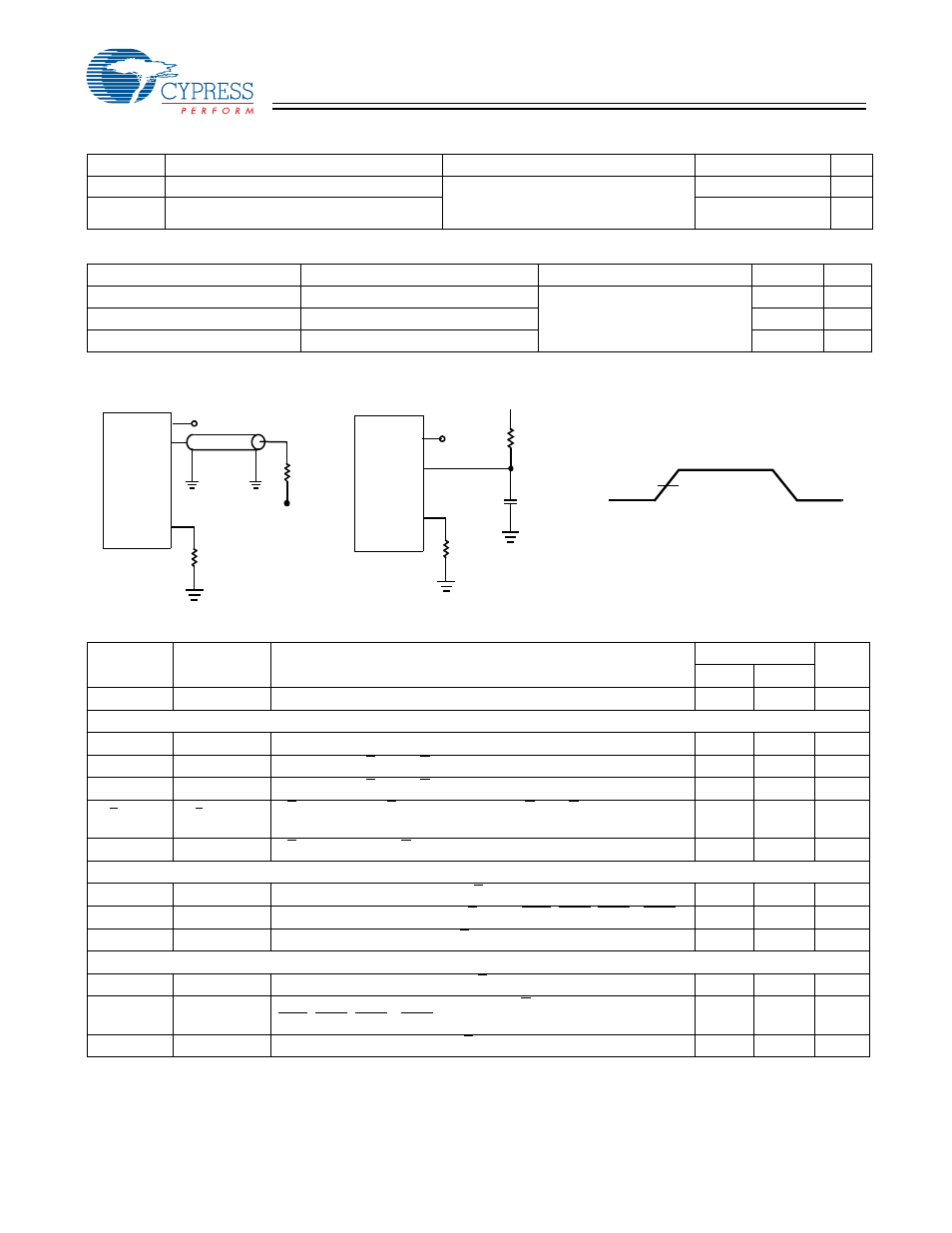
AC Test Loads and Waveforms
Switching Characteristics
Over the Operating Range
[21]
Cypress
Parameter
Consortium
Parameter
Description
167 MHz
Unit
Min.
Max.
t
Power
[22]
V
CC
(typical) to the First Access Read or Write
10
µs
Cycle Time
t
CYC
t
KHKH
K Clock and C Clock Cycle Time
6.0
ns
t
KH
t
KHKL
Input Clock (K/K and C/C) HIGH
2.4
ns
t
KL
t
KLKH
Input Clock (K/K and C/C) LOW
2.4
ns
t
KHKH
t
KHKH
K/K Clock Rise to K/K Clock Rise and C/C to C/C Rise (rising edge
to rising edge)
2.7
3.3
ns
t
KHCH
t
KHCH
K/K Clock Rise to C/C Clock Rise (rising edge to rising edge)
0.0
2.0
ns
Set-up Times
t
SA
t
SA
Address Set-up to Clock (K and K) Rise
0.7
ns
t
SC
t
SC
Control Set-up to Clock (K and K) Rise (RPS, WPS, BWS
0
, BWS
1
)
0.7
ns
t
SD
t
SD
D
[17:0]
Set-up to Clock (K and K) Rise
0.7
ns
Hold Times
t
HA
t
HA
Address Hold after Clock (K and K) Rise
0.7
ns
t
HC
t
HC
Control Signals Hold after Clock (K and K) Rise
(RPS, WPS, BWS
0
, BWS
1
)
0.7
ns
t
HD
t
HD
D
[17:0]
Hold after Clock (K and K) Rise
0.7
ns
Notes:
20. Tested initially and after any design or process change that may affect these parameters.
21. Unless otherwise noted, test conditions assume signal transition time of 2V/ns, timing reference levels of 0.75V,Vref = 0.75V, RQ = 250W, V
DDQ
= 1.5V, input
pulse levels of 0.25V to 1.25V, and output loading of the specified I
OL
/I
OH
and load capacitance shown in (a) of AC test loads.
22. This part has a voltage regulator that steps down the voltage internally; t
Power
is the time power needs to be supplied above V
DD
minimum initially before a read
or write operation can be initiated.
1.25V
0.25V
R = 50
Ω
5 pF
ALL INPUT PULSES
Device
R
L
= 50
Ω
Z
0
= 50
Ω
V
REF
= 0.75V
V
REF
= 0.75V
[21]
0.75V
Under
Test
0.75V
Device
Under
Test
OUTPUT
0.75V
V
REF
V
REF
OUTPUT
ZQ
ZQ
(a)
Slew Rate = 2 V/ns
RQ =
250
Ω
(b)
RQ =
250
Ω