Maximum ratings, Operating range, Electrical characteristics – Cypress CY7C1302DV25 User Manual
Page 13
CY7C1302DV25
Document #: 38-05625 Rev. *A
Page 13 of 18
Maximum Ratings
(Above which the useful life may be impaired.)
Storage Temperature ................................. –65°C to + 150°C
Ambient Temperature with
Power Applied............................................ –55°C to + 125°C
Supply Voltage on V
DD
Relative to GND....... –0.5V to + 3.6V
Supply Voltage on V
DDQ
Relative to GND ..... –0.5V to + V
DD
DC Applied to Outputs in High-Z......... –0.5V to V
DDQ
+ 0.5V
DC Input Voltage
[13
................................–0.5V to V
DD
+ 0.5V
Current into Outputs (LOW) .........................................20 mA
Static Discharge Voltage........................................... >2001V
(per MIL-STD-883, Method 3015)
Latch-up Current..................................................... >200 mA
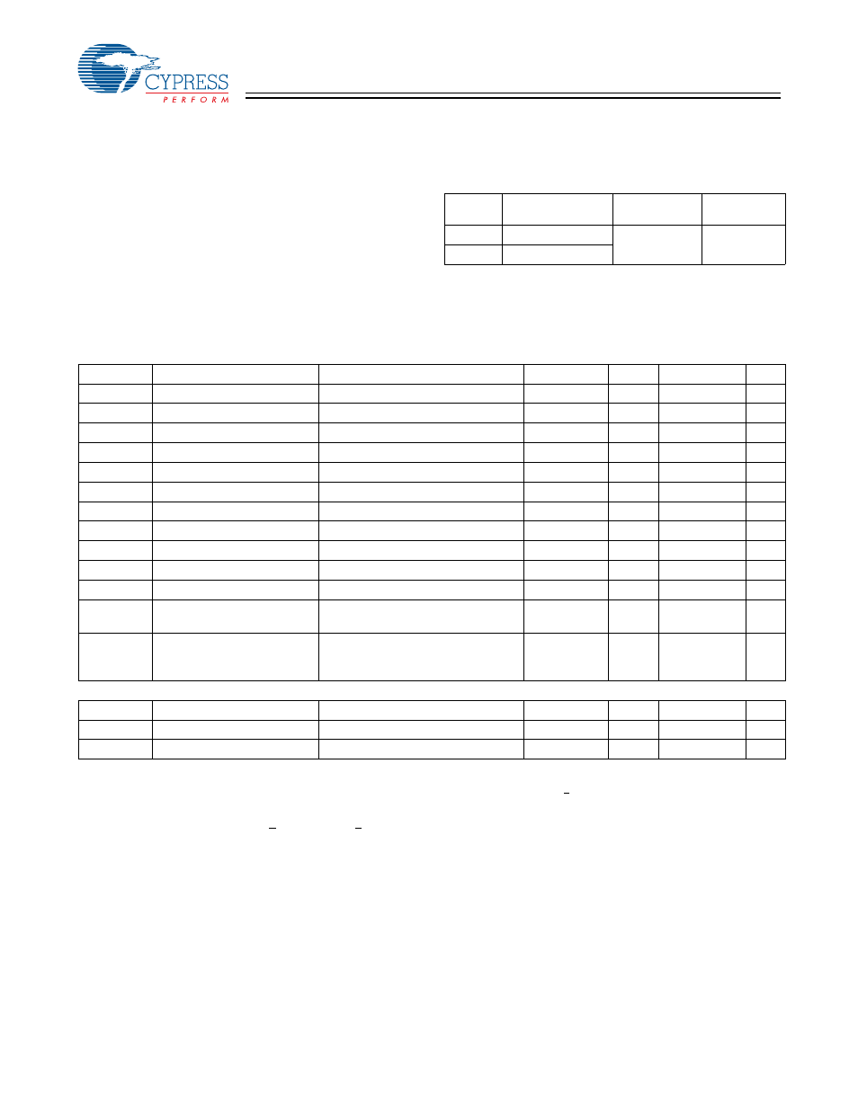
Operating Range
Range
Ambient
Temperature (T
A
)
V
DD
[14]
V
DDQ
[14]
Com’l
0°C to +70°C
2.5 ± 0.1V
1.4V to 1.9V
Ind’l
–40°C to +85°C
Electrical Characteristics
Over the Operating Range
[15]
DC Electrical Characteristics Over the Operating Range
Parameter
Description
Test Conditions
Min.
Typ.
Max.
Unit
V
DD
Power Supply Voltage
2.4
2.5
2.6
V
V
DDQ
I/O Supply Voltage
1.4
1.5
1.9
V
V
OH
Output HIGH Voltage
Note 16
V
DDQ
/2 – 0.12
V
DDQ
/2 + 0.12
V
V
OL
Output LOW Voltage
Note 17
V
DDQ
/2
– 0.12
V
DDQ
/2 + 0.12
V
V
OH(LOW)
Output HIGH Voltage
I
OH
= –0.1 mA, Nominal Impedance
V
DDQ
– 0.2
V
DDQ
V
V
OL(LOW)
Output LOW Voltage
I
OL
= 0.1 mA, Nominal Impedance
V
SS
0.2
V
V
IH
Input HIGH Voltage
[13]
V
REF
+ 0.1
V
DDQ
+ 0.3
V
V
IL
Input LOW Voltage
[13, 18]
–0.3
V
REF
– 0.1
V
I
X
Input Load Current
GND
≤ V
I
≤ V
DDQ
–5
5
µA
I
OZ
Output Leakage Current
GND
≤ V
I
≤ V
DDQ,
Output Disabled
–5
5
µA
V
REF
Input Reference Voltage
[19]
Typical value = 0.75V
0.68
0.75
0.95
V
I
DD
V
DD
Operating Supply
V
DD
= Max., I
OUT
= 0 mA,
f = f
MAX
= 1/t
CYC
500
mA
I
SB1
Automatic
Power-Down
Current
Max. V
DD
, Both Ports Deselected,
V
IN
≥ V
IH
or V
IN
≤ V
IL
, f =f
MAX
=1/t
CYC,
Inputs Static
240
mA
AC Input Requirements Over the Operating Range
Parameter
Description
Test Conditions
Min.
Typ.
Max.
Unit
V
IH
Input HIGH Voltage
V
REF
+ 0.2
–
V
V
IL
Input LOW Voltage
–
V
REF
– 0.2
V
Notes:
13. Overshoot: V
IH
(AC) < V
DDQ
+0.85V (Pulse width less than t
CYC
/2), Undershoot: V
IL(
AC) > –1.5V (Pulse width less than t
CYC
/2).
14. Power-up: Assumes a linear ramp from 0V to V
DD
(min.) within 200 ms. During this time V
IH
< V
DD
and V
DDQ
< V
DD
.
15. All voltage referenced to Ground.
16. Output are impedance controlled. I
OH
= –(V
DDQ
/2)/(RQ/5) for values of 175
Ω <= RQ <= 350Ω.
17. Output are impedance controlled. I
OL
= (V
DDQ
/2)/(RQ/5) for values of 175
Ω <= RQ <= 350Ω.
18. This spec is for all inputs except C and C Clock. For C and C Clock, V
IL
(Max.) = V
REF
– 0.2V.
19. V
REF
(Min.) = 0.68V or 0.46V
DDQ
, whichever is larger, V
REF
(Max.) = 0.95V or 0.54V
DDQ
, whichever is smaller.