8 peripheral connectors, Table 8-1: pmod header pin-out to fpga pins – Digilent 6005-210-000 User Manual
Page 7
The GPIO pins have an I/O level of 3.3V. They are controlled using the General
Purpose I/O IP included with the Xilinx EDK. Adding the IP to a project gives access
to two sets of two 32-bit software accessible registers at the base address of the GPIO
IP, each set consisting of a data register and a tri-state register. Each bit in the data
and tri-state register can be connected to a pin on the GPIO header. Writing a 1 to the
bit in the tri-state register configures the pin as input, while writing a 0 sets it to
output. Therefore, if the value of an input pin changes, its value in the data register
changes; conversely, writing a value to a data register bit will change the value of the
pin when configured as output.
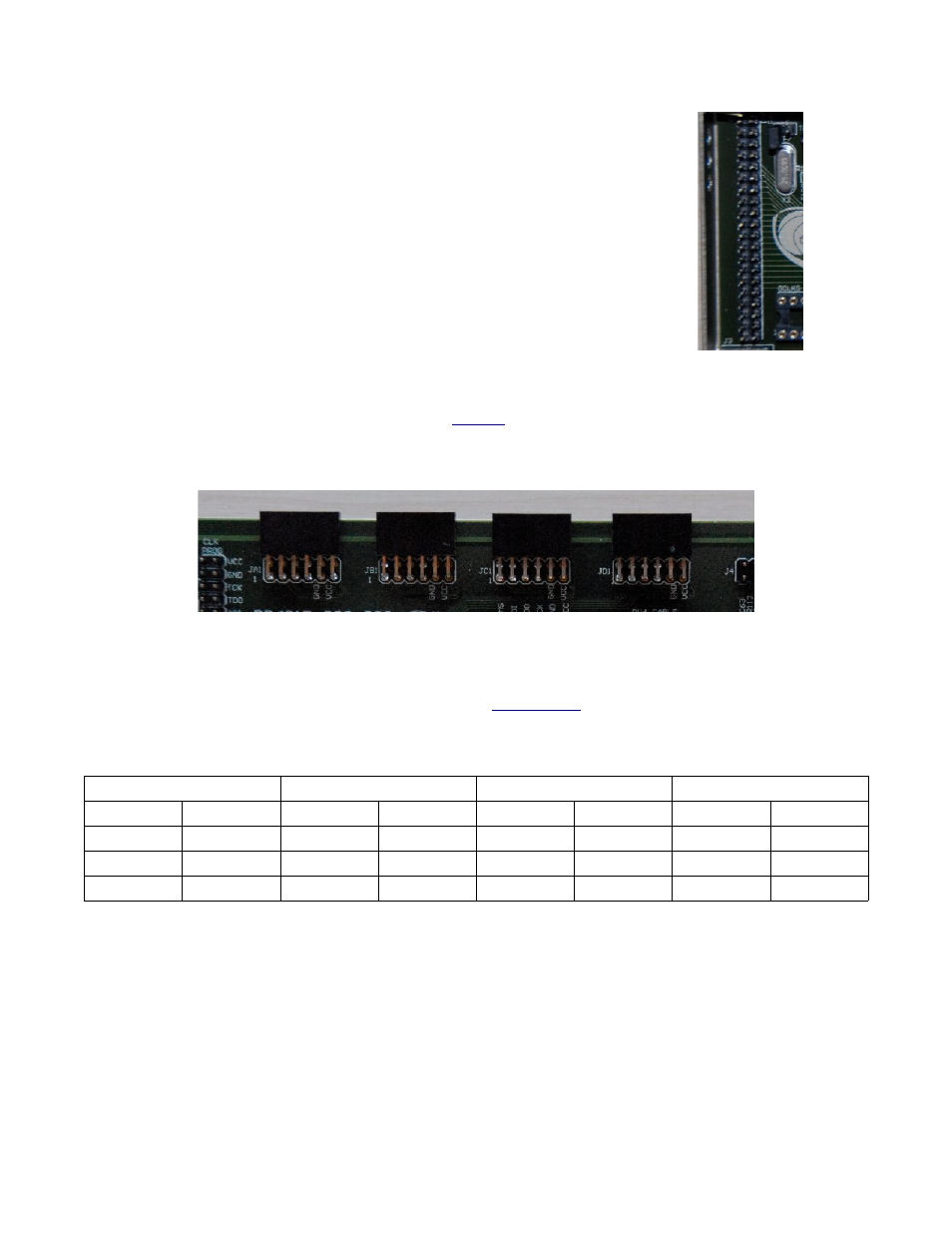
8 Peripheral Connectors
The Opus card has four two-row Pmod headers located along its top edge at positions JA1, JB1, JC1, and JD1. These
headers allow up to eight Pmods, such as those sold by
to be connected to the card at one time. These
headers greatly increase the usability of the card in a variety of applications by increasing the amount of user I/O
devices available.
Similar to the GPIO header, the Pmod headers have an I/O level of 3.3V, and are controlled by software-accessible
registers located at a base address generated by EDK during synthesis. The first 32 bits at the base address are the
data register for the Pmods, and the second 32 bits are the tri-state register. A reference design on using the Pmod
headers and software accessible registers can be found at the
The pin-out for the Pmod connectors is
shown in Table 8-1.
Table 8-1: Pmod Header Pin-out to FPGA Pins
Pmod 1: JA
Pmod 2: JB
Pmod 3: JC
Pmod 4: JD
JA1: C13
JA7: G12
JB1: C18
JB7: H19
JC1: C23
JC7: C24
JD1: B26
JD7: C26
JA2: C14
JA8: G14
JB2: C19
JB8: D19
JC2: D24
JC8: H11
JD2: D25
JD8: D26
JA3: G11
JA9: C16
JB3: D20
JB9: D21
JC3: F13
JC9: F14
JD3: G17
JD9: F18
JA4: H18
JA10: C17
JB4: C22
JB10: D23
JC4: F15
JC10: F17
JD4: G19
JD10: C21
Reference Manual
©
2010 Computer Measurement Laboratory
7 of 7