2 overview, Figure 2-1: opus card system block diagram – Digilent 6005-210-000 User Manual
Page 4
2 Overview
The Opus card is a complete development system driven by the Xilinx Virtex 5 FPGA. The card was designed with the
end-purpose of running as a standalone Linux system that plugs into a host PC and is a node in a network of Opus
systems. In addition to the node functionality, the Opus card also has all the necessary components to be an
independent development platform.
The Virtex 5 FPGA has powerful PowerPC 440 and MicroBlaze cores, and combined with 256 MB of DDR-2 RAM, the
Opus card can host a variety of applications, from peripheral management to full Linux kernels. Applications can be
loaded to the card using a JTAG port, or from the available Xilinx XCF32P Flash memory. The Opus card has four
peripheral module (Pmod) connectors that can host a variety of Pmod devices, such as LCD and seven segment
displays, LEDs, hardware adapters (PS/2, RS-232), and many others. A 2x20 GPIO header adds additional
input/output pins. The included Secure Digital port allows reading and writing to an SD filesystem, and the 10/100
Ethernet port provides the ability for the card to act as a network device.
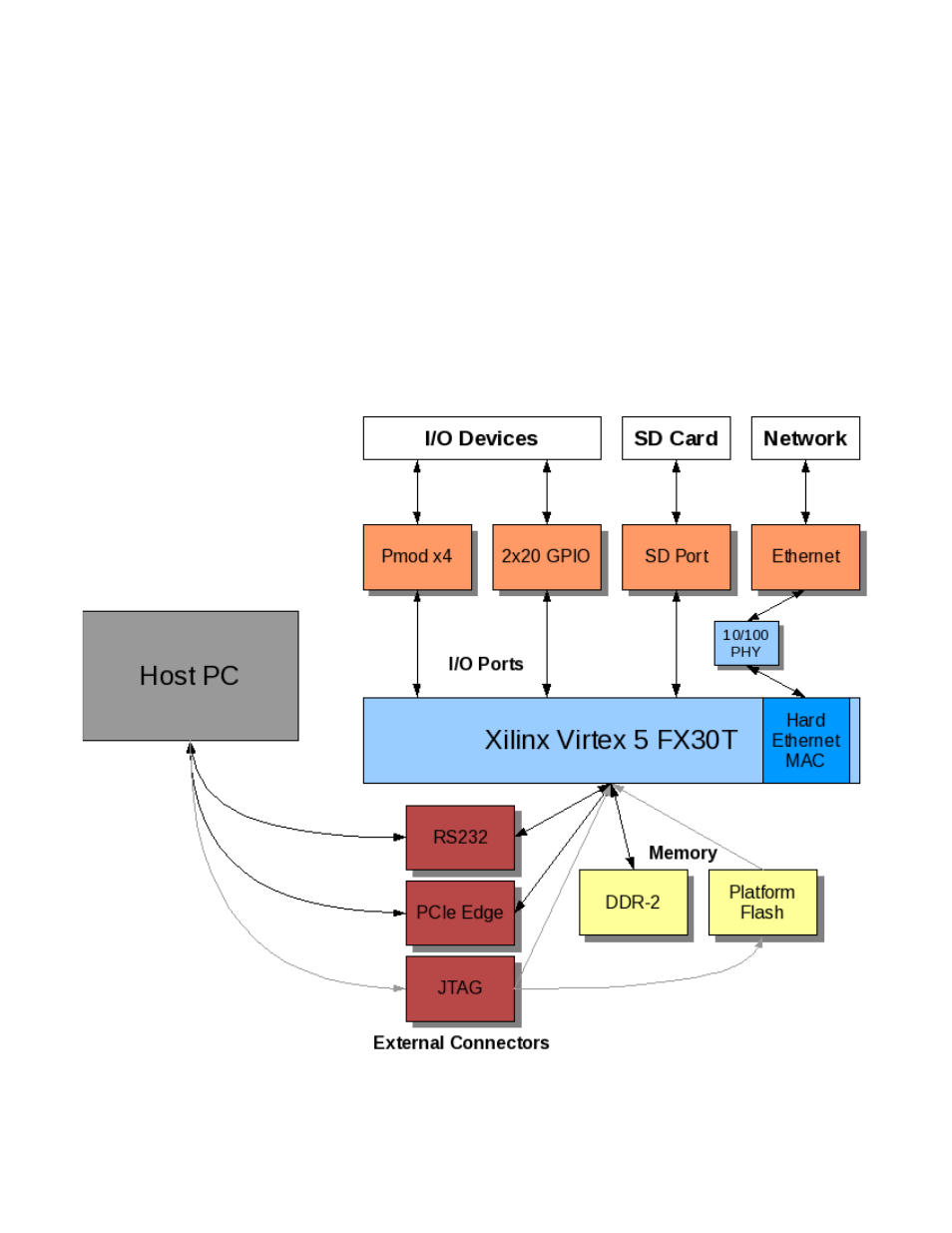
Figure 2-1 is a block diagram that represents the Opus card interfaced with a host system. The black arrows indicate
bi-directional communication, while the grey arrows are single direction.
Figure 2-1: Opus Card System Block Diagram
Reference Manual
©
2010 Computer Measurement Laboratory
4 of 7