3 power supply, 4 fpga and platform flash configuration, 5 clocks – Digilent 6005-210-000 User Manual
Page 5: 4 fpga and platorm flash confguraton
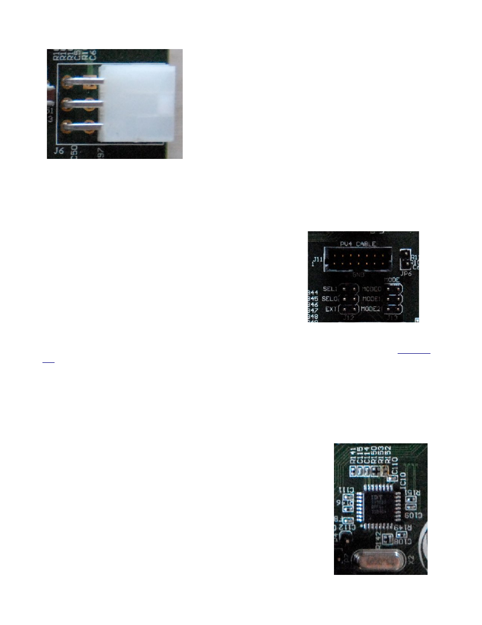
3 Power Supply
The Opus card requires a 12V 6-pin PCIe expansion card power source,
available on most modern power supply units. The socket on the card is
white in color and located in the upper right corner of the card, labeled
as J6. The power supply should be switched off while plugging in the
Opus card.
4 FPGA and Platorm Flash Confguraton
The Opus card must be configured before use. Configuration files, called bit files, can be generated from hardware
configurations and software applications built using the Xilinx EDK. The bit files can be loaded to the FPGA in two
ways: directly from a host PC through the JTAG port, or from the preloaded onboard Xilinx XCF16P platform flash
memory.
The location to load is selected by a mode jumper located at J13, directly
below the JTAG port. To configure the FPGA from JTAG, the mode jumpers
must remain open. In JTAG mode, the card will not perform any action
when turned on or reset, but waits for a configuration file to be loaded
using the Xilinx iMPACT tool. To configure the FPGA from platform flash,
jumper blocks must be placed across pins 1 and 2 (MODE 0) and 3 and 4
(MODE 1) of the mode jumper J13. When the jumpers are in place to use
the platform flash, the card will configure the FPGA from the bit file stored
in the platform flash when powered on or reset.
Please note: The Opus card platform flash is packaged with a configuration file already loaded. This configuration file
contains the manufacturing level hardware tests and Linux bootloader, and acts as a fail-safe configuration when
developing with the Opus card. If the platform flash is overwritten, the original bit file can be found at the
Also note, when in JTAG mode, the FPGA will retain the configuration file until a power cycle occurs or the reset
button is pressed at which point it will clear; alternately, the bit file remains in the platform flash unless it is
reprogrammed, and is unaffected by power cycles.
5 Clocks
The Opus card uses a programmable clock generator chip with eight outputs and available frequency ranges of 0.0049
– 550 MHz. The chip outputs three signal types: LVPECL, LVTTL, and LVDS. The chip has a 12-bit frequency multiplier,
and 8-bit pre and 12-bit post dividers.
The clock chip is programmed to the following frequencies during manufacturing:
•
Pin 6: 25.00 MHz
•
Pin 13: 25.00 MHz
•
Pin 29: 14.30 MHz
•
Pin 8: 12.00 MHz
•
Differential pair pins 10 and 11: 33.00 MHz
•
Differential pair pins 15 and 16: 100.00 MHz
Additionally, the 50 MHz oscillator frequency can be verified by measuring the
frequency at pin 3.
Reference Manual
©
2010 Computer Measurement Laboratory
5 of 7