Ethernet phy, Hdmi output – Digilent 410-258P-KIT User Manual
Page 4
Anvyl Reference Manual
www.digilentinc.com
page 4 of 16
Copyright Digilent, Inc. All rights reserved. Other product and company names mentioned may be trademarks of their respective owners.
DDR2 Memory
A single 1Gbit DDR2 memory chip is driven from the memory controller block in the Spartan-6 FGPA.
The DDR2 device, a MT47H64M16HR-25E or equivalent, provides a 16-bit bus and 64M locations.
The Anvyl board has been tested for DDR2 operation at up to an 800MHz data rate. The DDR2
interface follows the pin-out and routing guidelines specified in the Xilinx Memory Interface Generator
(MIG) User Guide. The interface supports SSTL18 signaling, and all address, data, clocks, and
control signals are delay-matched and impedance-controlled. Two well-matched DDR2 clock signal
pairs are provided so the DDR can be driven with low-skew clocks from the FPGA.
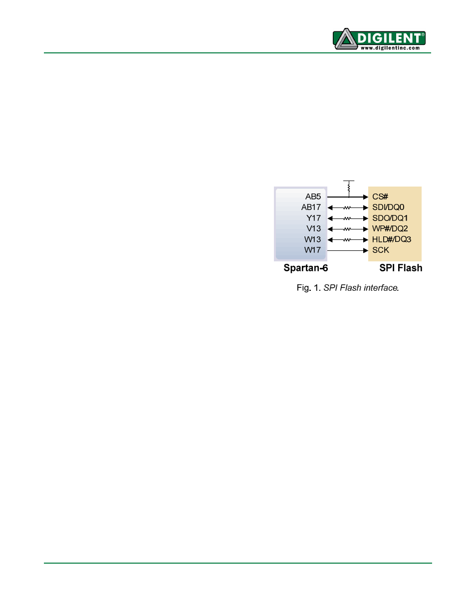
Flash Memory
The Anvyl board uses a 128Mbit Numonyx N25Q128
Serial flash memory device (organized as 16Mbit by 8) for
non-volatile storage of FPGA configuration files. The SPI
Flash can be programmed with a .mcs file using the
iMPACT software. An FPGA configuration file requires
less than 12Mbits, leaving 116Mbits available for user
data. Data can be transferred to and from a PC to/from
the flash device by user applications, or by facilities built
into the iMPACT PROM file generation software. User
designs programmed into the FPGA can also transfer
data to and from the flash.
A board test/demonstration program is loaded into the SPI Flash during manufacturing.
Ethernet PHY
The Anvyl board includes an SMSC 10/100 mbps PHY (LAN8720A-CP-TR) paired with a Halo
HFJ11-2450E RJ-45 connector. The PHY is connected to the FPGA using a RMII configuration. It is
configured to boot into “All Capable, with Auto Negotiation Enabled” mode on power-on. The data
sheet for the SMSC PHY is available from the SMSC website.
HDMI Output
The Anvyl board contains one unbuffered HDMI output port. The unbuffered port uses an HDMI type
A connector. Since the HDMI and DVI systems use the same TMDS signaling standard, a simple
adaptor (available at most electronics stores) can be used to drive a DVI connector from the HDMI
output port. The HDMI connector does not include VGA signals, so analog displays cannot be driven.
The 19-pin HDMI connectors include four differential data channels, five GND connections, a one-wire
Consumer Electronics Control (CEC) bus, a two-wire Display Data Channel (DDC) bus that is
essentially an I
2
C bus, a Hot Plug Detect (HPD) signal, a 5V signal capable of delivering up to 50mA,
and one reserved (RES) pin. Of these, the differential data channels, I
2
C bus, and CEC are connected
to the FPGA.