Oscillators/clocks – Digilent 410-258P-KIT User Manual
Page 13
Anvyl Reference Manual
www.digilentinc.com
page 13 of 16
Copyright Digilent, Inc. All rights reserved. Other product and company names mentioned may be trademarks of their respective owners.
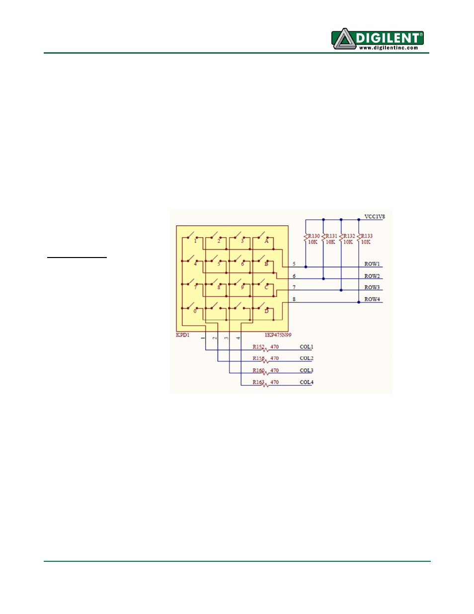
gives the user four row pins and four column pins to address a button push. When a button is
pressed, the pins corresponding to that button’s row and column are connected.
To read a button’s state, the column pin in which the button resides must be driven low while the other
three column pins are driven high. This enables all of the buttons in that column. When a button in
that column is pushed, the corresponding row pin will read logic low.
The state of all 16 buttons can be determined in a four-step process by enabling each of the four
columns one at a time. This can be accomplished by rotating an “1110” pattern through the column
pins. During each step, the logic levels of the row pins correspond to the state of the buttons in that
column.
To allow simultaneous button presses in the same row, instead configure the column pins as bi-
directional with internal pull-up resistors and keep the columns not currently being read at high
impedance.
Fig. 13. Keypad schematic
Oscillators/Clocks
The Anvyl board includes a single 100MHz Crystal oscillator connected to pin D11 (D11 is a GCLK
input in bank 0). The input clock can drive any or all of the four clock management tiles in the Spartan-
6. Each tile includes two Digital Clock Managers (DCMs) and one Phase-Locked Loop (PLLs).DCMs
provide the four phases of the input frequency (0º, 90º, 180º, and 270º), a divided clock that can be
the input clock divided by any integer from 2 to 16 or 1.5, 2.5, 3.5... 7.5, and two antiphase clock
outputs that can be multiplied by any integer from 2 to 32 and simultaneously divided by any integer
from 1 to 32.
PLLs use Voltage Controlled Oscillators (VCOs) that can be programmed to generate frequencies in
the 400MHz to 1080MHz range by setting three sets of programmable dividers during FPGA
Keypad Pinout
ROW1:
E4
ROW2:
F3
ROW3:
G8
ROW4:
G7
COL1:
H8
COL2:
J7
COL3:
K8
COL4:
K7