Switching characteristics, In the – Cypress Perform CY7C1513KV18 User Manual
Page 24
CY7C1511KV18, CY7C1526KV18
CY7C1513KV18, CY7C1515KV18
Document Number: 001-00435 Rev. *E
Page 24 of 31
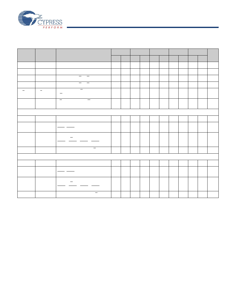
Switching Characteristics
Over the Operating Range
Cypress
Parameter
Consortium
Parameter
Description
333 MHz
300 MHz
250 MHz
200 MHz
167 MHz
Unit
Min Max Min Max Min Max Min Max Min Max
t
POWER
V
DD
(Typical) to the First Access
1
1
1
1
1
ms
t
CYC
t
KHKH
K Clock and C Clock Cycle Time
3.0
8.4
3.3
8.4
4.0
8.4
5.0
8.4
6.0
8.4
ns
t
KH
t
KHKL
Input Clock (K/K; C/C) HIGH
1.20
–
1.32
–
1.6
–
2.0
–
2.4
–
ns
t
KL
t
KLKH
Input Clock (K/K; C/C) LOW
1.20
–
1.32
–
1.6
–
2.0
–
2.4
–
ns
t
KHKH
t
KHKH
K Clock Rise to K Clock Rise and C
to C Rise (rising edge to rising edge)
1.35
–
1.49
–
1.8
–
2.2
–
2.7
–
ns
t
KHCH
t
KHCH
K/K Clock Rise to C/C Clock Rise
(rising edge to rising edge)
0
1.30
0
1.45
0
1.8
0
2.2
0
2.7
ns
Setup Times
t
SA
t
AVKH
Address Setup to K Clock Rise
0.4
–
0.4
–
0.5
–
0.6
–
0.7
–
ns
t
SC
t
IVKH
Control Setup to K Clock Rise
(RPS, WPS)
0.4
–
0.4
–
0.5
–
0.6
–
0.7
–
ns
t
SCDDR
t
IVKH
Double Data Rate Control Setup to
Clock (K/K) Rise
(BWS
0
, BWS
1
,
BWS
2
, BWS
3
)
0.3
–
0.3
–
0.35
–
0.4
–
0.5
–
ns
t
SD
t
DVKH
D
[X:0]
Setup to Clock (K/K) Rise
0.3
–
0.3
–
0.35
–
0.4
–
0.5
–
ns
Hold Times
t
HA
t
KHAX
Address Hold after K Clock Rise
0.4
–
0.4
–
0.5
–
0.6
–
0.7
–
ns
t
HC
t
KHIX
Control Hold after K Clock Rise
(RPS, WPS)
0.4
–
0.4
–
0.5
–
0.6
–
0.7
–
ns
t
HCDDR
t
KHIX
Double Data Rate Control Hold after
Clock (K/K) Rise
(BWS
0
, BWS
1
, BWS
2
, BWS
3
)
0.3
–
0.3
–
0.35
–
0.4
–
0.5
–
ns
t
HD
t
KHDX
D
[X:0]
Hold after Clock (K/K) Rise
0.3
–
0.3
–
0.35
–
0.4
–
0.5
–
ns
Notes
23. When a part with a maximum frequency above 167 MHz is operating at a lower clock frequency, it requires the input timings of the frequency range in which it is operated
and outputs data with the output timings of that frequency range.
24. This part has a voltage regulator internally; t
POWER
is the time that the power must be supplied above V
DD
minimum initially before a read or write operation is initiated.