Application example, Truth table – Cypress Perform CY7C1513KV18 User Manual
Page 10
CY7C1511KV18, CY7C1526KV18
CY7C1513KV18, CY7C1515KV18
Document Number: 001-00435 Rev. *E
Page 10 of 31
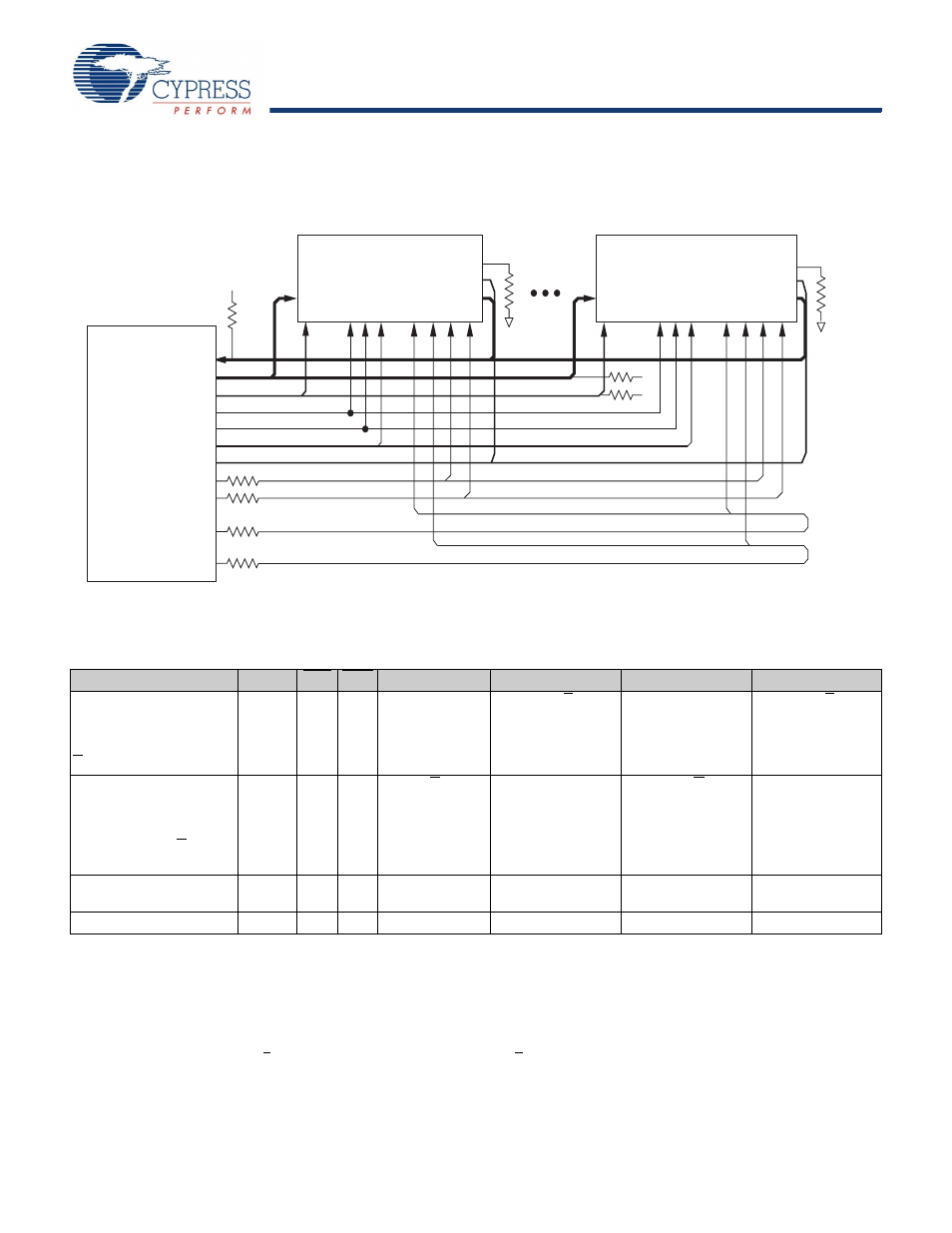
Application Example
shows four QDR-II used in an application.
Figure 1. Application Example
Truth Table
The truth table for CY7C1511KV18, CY7C1526KV18, CY7C1513KV18, and CY7C1515KV18 follows.
Operation
K
RPS WPS
DQ
DQ
DQ
DQ
Write Cycle:
Load address on the rising
edge of K; input write data
on two consecutive K and
K rising edges.
L-H
H
[8]
L
D(A) at K(t + 1)
↑ D(A + 1) at K(t + 1)↑ D(A + 2) at K(t + 2)↑ D(A + 3) at K(t + 2)↑
Read Cycle:
Load address on the rising
edge of K; wait one and a
half cycle; read data on
two consecutive C and C
rising edges.
L-H
L
X
Q(A) at C(t + 1)
↑ Q(A + 1) at C(t + 2)↑ Q(A + 2) at C(t + 2)↑ Q(A + 3) at C(t + 3)↑
NOP: No Operation
L-H
H
H
D = X
Q = High-Z
D = X
Q = High-Z
D = X
Q = High-Z
D = X
Q = High-Z
Standby: Clock Stopped
Stopped
X
X
Previous State
Previous State
Previous State
Previous State
R = 250
ohms
Vt
R
R = 250
ohms
Vt
Vt
R
Vt = Vddq/2
R = 50
ohms
R
C C#
D
A
SRAM #4
R
P
S
#
W
P
S
#
B
W
S
#
K
ZQ
CQ/CQ#
Q
K#
C C#
D
A
K
SRAM #1
R
P
S
#
W
P
S
#
B
W
S
#
ZQ
CQ/CQ#
Q
K#
BUS
MASTER
(CPU
or
ASIC)
DATA IN
DATA OUT
Address
RPS#
WPS#
BWS#
Source K
Source K#
Delayed K
Delayed K#
CLKIN/CLKIN#
Notes
2. X = “Don't Care,” H = Logic HIGH, L = Logic LOW,
↑
represents rising edge.
3. Device powers up deselected with the outputs in a tristate condition.
4. “A” represents address location latched by the devices when transaction was initiated. A + 1, A + 2, and A +3 represents the address sequence in the burst.
5. “t” represents the cycle at which a read/write operation is started. t + 1, t + 2, and t + 3 are the first, second and third clock cycles respectively succeeding the “t” clock cycle.
6. Data inputs are registered at K and K rising edges. Data outputs are delivered on C and C rising edges, except when in single clock mode.
7. Ensure that when the clock is stopped K = K and C = C = HIGH. This is not essential, but permits most rapid restart by overcoming transmission line charging
symmetrically.
8. If this signal was LOW to initiate the previous cycle, this signal becomes a “Don’t Care” for this operation.
9. This signal was HIGH on previous K clock rise. Initiating consecutive read or write operations on consecutive K clock rises is not permitted. The device ignores the
second read or write request.