Kontron COMe-bCD2 User Manual
Page 27
4 Connector Pinouts
Kontron User's Guide ETXexpress® CD
27
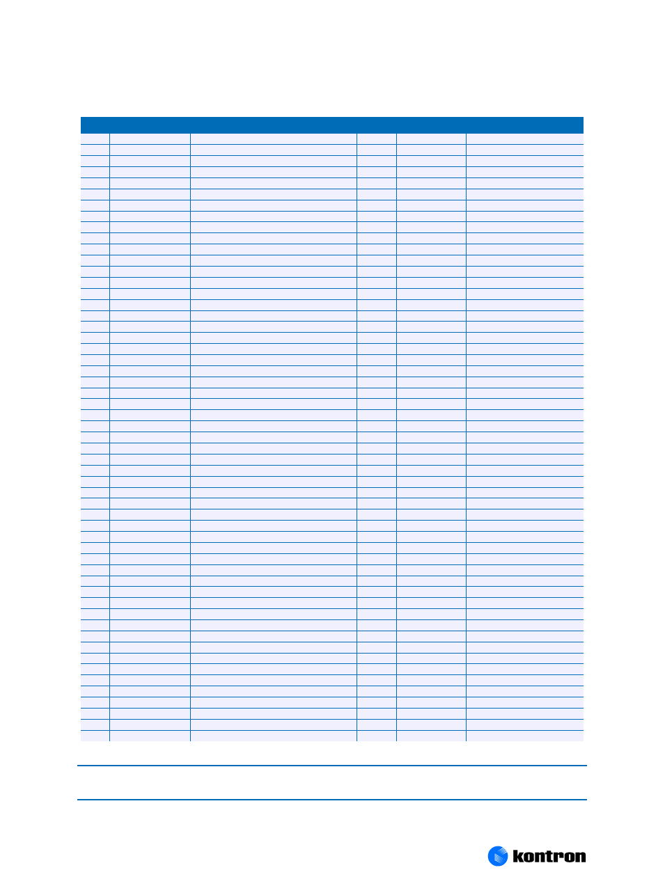
Connector X1B (Signal Levels D1-D55)
Pin D1-D55
[
LAN
|
Power
|
USB
|
SATA
|
PCIe
|
AUDIO
|
LPC
]
Pin
Signal
Description
Type
Termination
Comment
D1
GND
Power Ground
PWR
-
-
D2
IDE_D5
IDE Data Bus
IO
-
-
D3
IDE_D10
IDE Data Bus
IO
-
-
D4
IDE_D11
IDE Data Bus
IO
-
-
D5
IDE_D12
IDE Data Bus
IO
-
-
D6
IDE_D4
IDE Data Bus
IO
-
-
D7
IDE_D0
IDE Data Bus
IO
-
-
D8
IDE_REQ
IDE Data Bus
IO
-
-
D9
IDE_IOW#
IDE IO Write
O-3,3
-
-
D10
IDE_ACK#
IDE DMA Acknowledge
O-3,3
-
-
D11
GND
Power Ground
PWR
-
-
D12
IDE_IRQ
IDE Interrupt Request
I-3,3
PU 8k2 3,3V
-
D13
IDE_A0
IDE Adress Bus
O-3,3
-
-
D14
IDE_A1
IDE Adress Bus
O-3,3
-
-
D15
IDE_A2
IDE Adress Bus
O-3,3
-
-
D16
IDE_CS1#
IDE Chip Select Channel 0
O-3,3
-
-
D17
IDE_CS3#
IDE Chip Select Channel 1
O-3,3
-
-
D18
IDE_RESET#
IDE Hard Drive Reset
O-3,3
-
-
D19
PCI_GNT3#
PCI Bus Grant 3
O-3,3
-
-
D20
PCI_REQ3#
PCI Bus Reqest 0
I-3,3
PU 8k2 3,3V
-
D21
GND
Power Ground
PWR
-
-
D22
PCI_AD1
PCI Adress & Data Bus line
IO-3,3
-
-
D23
PCI_AD3
PCI Adress & Data Bus line
IO-3,3
-
-
D24
PCI_AD5
PCI Adress & Data Bus line
IO-3,3
-
-
D25
PCI_AD7
PCI Adress & Data Bus line
IO-3,3
-
-
D26
PCI_C/BE0#
PCI Bus Command and Byte enables 0
IO-3,3
-
-
D27
PCI_AD9
PCI Adress & Data Bus line
IO-3,3
-
-
D28
PCI_AD11
PCI Adress & Data Bus line
IO-3,3
-
-
D29
PCI_AD13
PCI Adress & Data Bus line
IO-3,3
-
-
D30
PCI_AD15
PCI Adress & Data Bus line
IO-3,3
-
-
D31
GND
Power Ground
PWR
-
-
D32
PCI_PAR
PCI Bus Parity
IO-3,3
-
-
D33
PCI_SERR#
PCI Bus System Error
IO-3,3
PU 8k2 3,3V
-
D34
PCI_STOP#
PCI Bus Stop
IO-3,3
PU 8k2 3,3V
-
D35
PCI_TRDY#
PCI Bus Target Ready
IO-3,3
PU 8k2 3,3V
-
D36
PCI_FRAME#
PCI Bus Cycle Frame
IO-3,3
PU 8k2 3,3V
-
D37
PCI_AD16
PCI Adress & Data Bus line
IO-3,3
-
-
D38
PCI_AD18
PCI Adress & Data Bus line
IO-3,3
-
-
D39
PCI_AD20
PCI Adress & Data Bus line
IO-3,3
-
-
D40
PCI_AD22
PCI Adress & Data Bus line
IO-3,3
-
-
D41
GND
Power Ground
PWR
-
-
D42
PCI_AD24
PCI Adress & Data Bus line
IO-3,3
-
-
D43
PCI_AD26
PCI Adress & Data Bus line
IO-3,3
-
-
D44
PCI_AD28
PCI Adress & Data Bus line
IO-3,3
-
-
D45
PCI_AD30
PCI Adress & Data Bus line
IO-3,3
-
-
D46
PCI_IRQC#
PCI Bus Interrupt Request C
I-3,3
PU 8k2 3,3V
-
D47
PCI_IRQD#
PCI Bus Interrupt Request D
I-3,3
PU 8k2 3,3V
-
D48
PCI_CLKRUN#
PCI Clock Run
I-3,3
PU 10k 3,3V
-
D49
PCI_M66EN
n.c.
nc
-
-
D50
PCI_CLK
PCI Clock
O-3,3
-
-
D51
GND
Power Ground
PWR
-
-
D52
PEG_TX0+
PCIexpress Graphics Transmit + (0)
I
-
DVOBD8
D53
PEG_TX0-
PCIexpress Graphics Transmit - (0)
I
-
DVOBD9
D54
PEG_LANE_RV#
PCIexpress Graphics Lane Reversal
I
-
-
D55
PEG_TX1+
PCIexpress Graphics Transmit + (1)
I
-
-
Note:
The termination resistors in this table are already mounted on the COM Express® board. Refer to the design
guide for information about additional termination resistors.