Pin configuration, Ata6264 [preliminary – Atmel ATA6264 User Manual
Page 4
4
4929B–AUTO–01/07
ATA6264 [Preliminary]
2.
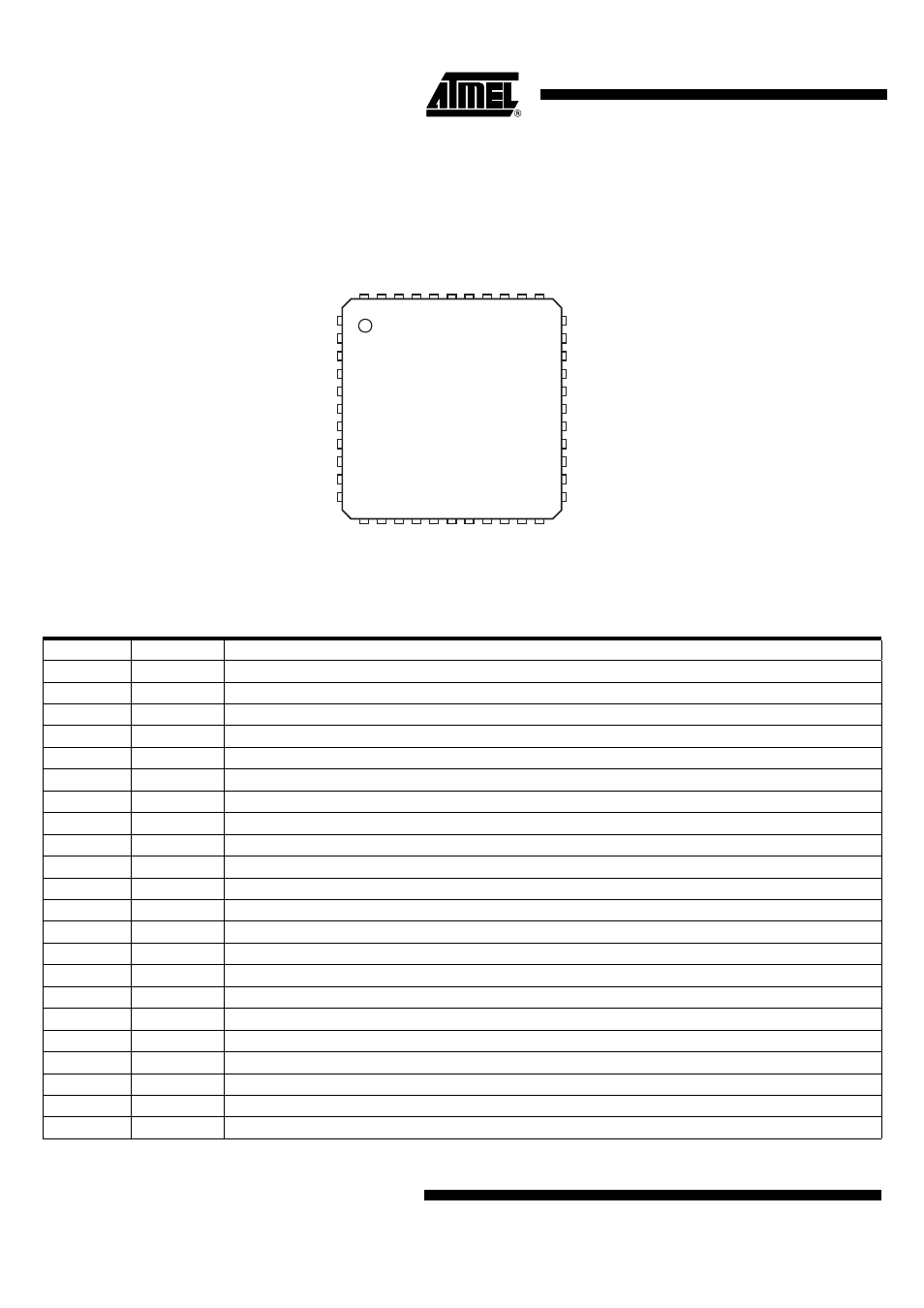
Pin Configuration
Figure 2-1.
Pinning QFP44
K15
EVZ
VSAT
GNDD
VINT
COMSATI
SVPERI
VPERI
GNDA
VCORE
SVSAT
USP
K30
K2
IASG1
IASG2
IASG3
ISENS
TxD1
IASG5
IASG4
K1
RESQ
RxD2
RxD1
TxD2
MISO
SSQ
SCLK
MOSI
RESQ2
IREF
UZP
COMEVZO
GNDB
GEVZ
OCEVZ
FBEVZ
CP
SVCORE
CP-OUT
COMCOO
COMCOI
COMSATO
1
2
3
4
9
10
11
5
6
8
7
33
32
31
30
25
24
23
29
28
26
27
44 43 42 41
35 34
36
38 37
39
40
12 13 14 15
21 22
20
18 19
17
16
Table 2-1.
Pin Description
Pin
Symbol
Function
1
USP
Comparator input
2
K30
Continuous connection to the car battery
3
K1
Bus line of 1
st
ISO9141 interface
4
K2
Bus line of 2
nd
ISO9141 interface
5
IASG1
Output of voltage source 1
6
IASG2
Output of voltage source 2
7
IASG3
Output of voltage source 3
8
IASG4
Output of voltage source 4
9
IASG5
Output of voltage source 5
10
ISENS
Output of the current mirror from the IASGx interface
11
TXD1
Data input of the 1
st
ISO9141 interface
12
RESQ
Reset output
13
RXD2
Data output of the 2
nd
ISO9141 interface
14
RXD1
Data output of the 1
st
ISO9141 interface
15
TXD2
Data input of the 2
nd
ISO9141 interface
16
MISO
Data output of the serial interface
17
SSQ
Chip select of the serial interface
18
SCLK
Clock input of the serial interface
19
MOSI
Data input of the serial Interface
20
RESQ2
Redundant reset output
21
IREF
Connection for the external reference resistor
22
UZP
Analog measurement output