Ata6264 [preliminary – Atmel ATA6264 User Manual
Page 36
36
4929B–AUTO–01/07
ATA6264 [Preliminary]
Necessary for operation:
V
EVZ
= 5.5V to 40V or V
K30
= 5.5V to 40V, V
CP
> V
EVZ
+ 7V or V
CP
> V
K30
+ 7V,
V
PERI
> V
CORE
– 0.3V, V
INT
= 3.7V to 5.47V
Operating conditions of all other supply pins:
V
SAT
is within functional range limits, T
j
= –40°C to 150°C
Other pins:
As defined in
Section 4. ”Functional Range” on page 8
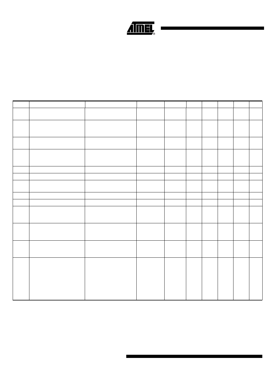
Table 12-1.
Electrical Characteristics – VCORE Power Supply
No.
Parameters
Test Conditions
Pin
Symbol
Min
Typ.
Max.
Unit
Type*
11.1
V
EVZ
voltage for the VCORE
regulator to start running
Initial programming:
V
VCORE
= 5V or 2.5V
EVZ
V
EVZ
7.5
9
V
A
11.1a
V
VPERI
voltage for the
VCORE regulator to start
running
Initial programming:
V
VCORE
= 1.88V
VPERI
V
VPERI
1.25
1.7
V
A
11.2
V
EVZ
voltage for the VCORE
regulator to stop running
Initial programming:
V
VCORE
= 5V or 2.5V
EVZ
V
EVZ
5.5 6.2
V
A
11.2a
Hysteresis at VPERI for the
VCORE regulator to stop
running
Initial programming:
V
VCORE
= 1.88V
VPERI
V
HYS
50
150
mV
A
11.3
Switch-on time via pin EVZ
SVCORE
t
SVCORE
0
20
µs
A
11.4
Switch-off time via pin EVZ
SVCORE
t
SVCORE
0
10
µs
A
11.5
Regulator switching
frequency
See numbers 8.1 and 8.2
of
SVCORE
f
SVCORE
A
11.6
Output current limit
SVCORE
I
SVCORE
0.7
0.9
A
A
11.7
R
Dson
of output transistor
SVCORE
R
SVCORE
1.2
Ω
A
11.8
Output voltage #1
V
VCORE1
programmed,
band-gap tolerance
included
VCORE
V
VCORE1
–4%
5.0
+4%
V
A
11.9
Output voltage #2
V
VCORE2
programmed,
band-gap tolerance
included
VCORE
V
VCORE2
–4%
2.5
+4%
V
A
11.10
Output voltage #3
V
VCORE3
programmed,
band-gap tolerance
included
VCORE
V
VCORE3
–4%
1.88
+4%
V
A
11.11
Output transistor switch-on
time
Time between reaching
0.1
×
(V
K30max
– V
VCOREmin
)
and
0.9
×
(V
K30max
– V
VCOREmin
)
or
0.1
×
(V
EVZmax
– V
VCOREmin
)
and
0.9
×
(V
EVZmax
– V
VCOREmin
)
SVORE
t
SVCOREon
150
ns
A
*) Type means: A = 100% tested, B = 100% correlation tested, C = Characterized on samples, D = Design parameter
Notes:
1. Depending on implementation of slope compensation, sub-harmonics have to be prevented.
2. The value of the minimum load current must be higher than the internal pull-up current at pin VCORE to ensure proper
function of the regulator.