Ata6264 [preliminary – Atmel ATA6264 User Manual
Page 32
32
4929B–AUTO–01/07
ATA6264 [Preliminary]
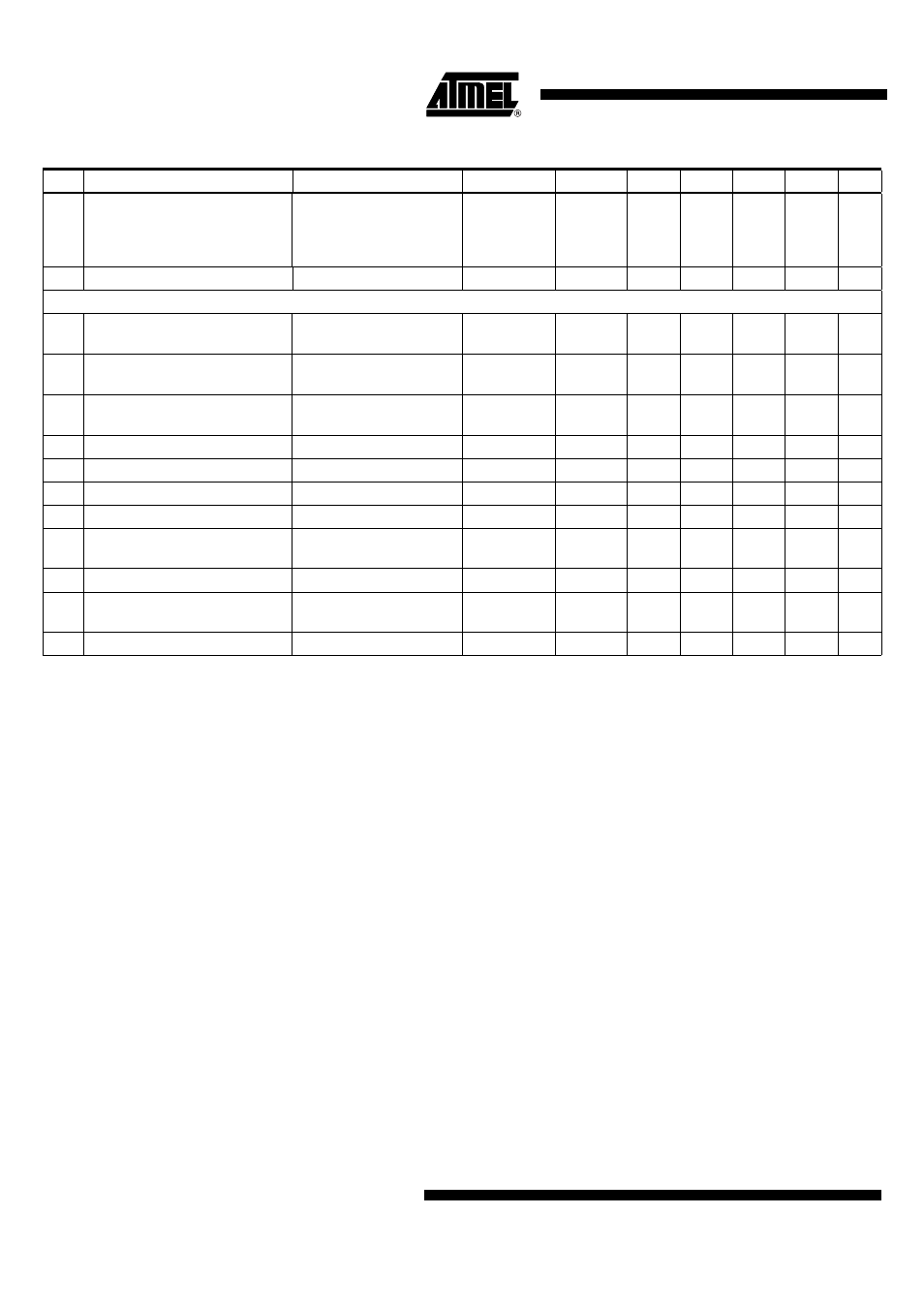
9.15 Overcurrent switch-on time
Time between reaching
overcurrent and reaching
90% of V
SVSAT
maximum
under on condition
SVSAT
t
SVSAToff
0
0.5
µs
A
9.16 Leakage current at pin SVSAT
Output transistor off
SVSAT
I
SVSAT
–10
+10
µA
A
Error Amplifier
9.17
Maximum output current at pin
COMSATO sinking to low
COMSATO
I
COMSATO
200
3000
µA
A
9.18
Maximum output current at pin
COMSATO sourcing to high
COMSATO
I
COMSATO
–165
–85
µA
A
9.19
Input impedance at pin
COMSATI
COMSATI
R
COMSATI
9
23
k
Ω
A
9.20 Input offset voltage
–10
+10
mV
D
9.21 DC open-loop gain
70
dB
D
9.22 Unity-gain bandwidth
2
MHz
D
9.23 Output voltage low
I
COMSATO
= 165 µA
COMSATO
V
COMSATO
0
0.3
V
A
9.24 Output voltage high
I
COMSATO
= –85 µA
COMSATO
V
COMSATO
V
VINT
–
0.6V
V
VINT
V
A
9.25 Leading-edge blanking time
t
blank
150
200
ns
D
9.26
Slope of artificial ramp for slope
compensation
dV/dt
150
(1)
240
(1)
mV/µs
D
9.27 VSAT loss detection threshold
(2)
I
Load
0
1.5
mA
D
Table 10-1.
Electrical Characteristics (Continued)– VSAT Power Supply
No. Parameters
Test Conditions
Pin
Symbol
Min
Typ.
Max.
Unit
Type*
*) Type means: A = 100% tested, B = 100% correlation tested, C = Characterized on samples, D = Design parameter
Notes:
1. Depending on implementation of slope compensation; sub-harmonics must be prevented
2. The value of the minimum load current must be higher than the internal pull-up current at pin VSAT to ensure proper func-
tion of the regulator