Cirrus Logic CDB5484U User Manual
Features, General description
Copyright
Cirrus Logic, Inc. 2012
(All Rights Reserved)
Cirrus Logic, Inc.
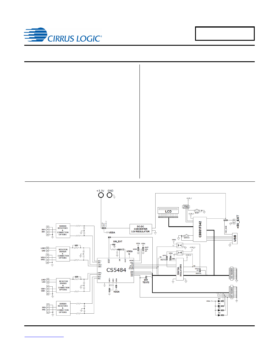
CDB5484U
CDB5484U Engineering Board and GUI Software
Features
• Standalone Power Meter Application
• Voltage and Current Interfaces
• Low- and High-voltage Sensor Connections
• Adaptable Sensor Filters Onboard
• USB Communication with PC
• UART/SPI Isolated Communication
• Onboard C8051F342 Microcontroller
• Single Supply Operation from USB or an External +5V DC
Supply
• Onboard DC-DC Converter and Regulator
• LCD Power Monitor Display
• LabWindows
®
/CVI
®
GUI Software
– Full Register Setup and Chip Control
– Simplified Register
– Quick Calibration Control
– FFT Analysis
– Time Domain Analysis
– Noise Histogram Analysis
• Voltage Reference Access
General Description
The CDB5484U is an extensive tool designed to evaluate the
functionality and performance of Cirrus Logic’s CS5484 pow-
er/energy measurement device.
Multiple analog input connection options, configuration input fil-
ters, direct and isolated digital interfaces, multiple power supply
options, an onboard programmable microcontroller, and visual
LEDs with an LCD panel make the board a flexible and powerful
customer development tool for various power/energy measure-
ment applications.
The GUI software provides easy and complete access and con-
trol to the onboard CS5484 device. It also includes the function
of raw ADC data collection with time domain, frequency domain,
and histogram analysis.
Schematics in the PADS™ PowerLogic™ format are available
on request.
ORDERING INFORMATION
CDB5484U-Z
Evaluation Board
APR’12
DS919DB5
Document Outline
- Features
- Table of Contents
- List of Figures
- 1. Hardware
- 2. Software
- 2.1 Installation Procedure
- 2.2 Using the Software
- 2.3 Start-up Window
- 2.4 Connect Menu
- 2.5 System Menu
- 2.5.1 Setup Window
- 2.5.1.1 Refresh Screen Button
- 2.5.1.2 Reset DUT Button
- 2.5.1.3 Save Config and Load Config Buttons
- 2.5.1.4 CS5484 MCLK Frequency
- 2.5.1.5 Configuration Registers
- 2.5.1.6 Pulse Control Register
- 2.5.1.7 Pulse Width and Pulse Rate Registers
- 2.5.1.8 Phase Compensation
- 2.5.1.9 Integrator Gain, System Gain
- 2.5.1.10 Sample Count, Cycle Count, Settle Time
- 2.5.1.11 Epsilon
- 2.5.1.12 ZXNUM
- 2.5.1.13 Mask Register
- 2.5.1.14 Temperature Registers
- 2.5.1.15 V / I Zero-crossing Level and No Load Threshold
- 2.5.1.16 V1/V2 Sag, V1/ V2 Swell, and I1/I2 Overcurrent Registers
- 2.5.1.17 Register Checksum, SerialCtrl Registers
- 2.5.1 Setup Window
- 2.6 Calibration Window
- 2.7 Conversion Window
- 2.8 Cirrus Test Window
- 2.8.1 Data Collection Window
- 2.8.1.1 Time Domain / FFT / Histogram Selector
- 2.8.1.2 Config Button
- 2.8.1.3 Collect Button
- 2.8.1.4 Output Button
- 2.8.1.5 Zoom Button
- 2.8.1.6 Channel Select Button
- 2.8.1.7 Output Button and Window
- 2.8.1.8 Configuration Window
- 2.8.1.9 Collecting Data Sets
- 2.8.1.10 Analyzing Data
- 2.8.1.11 Histogram Information
- 2.8.1.12 Frequency Domain Information
- 2.8.1.13 Time Domain Information
- 2.8.2 Data Collection to File Window
- 2.8.3 Setup and Test Window
- 2.8.1 Data Collection Window
- Appendix A. Bill of Materials
- Appendix B. Schematics
- Appendix C. Layer Plots