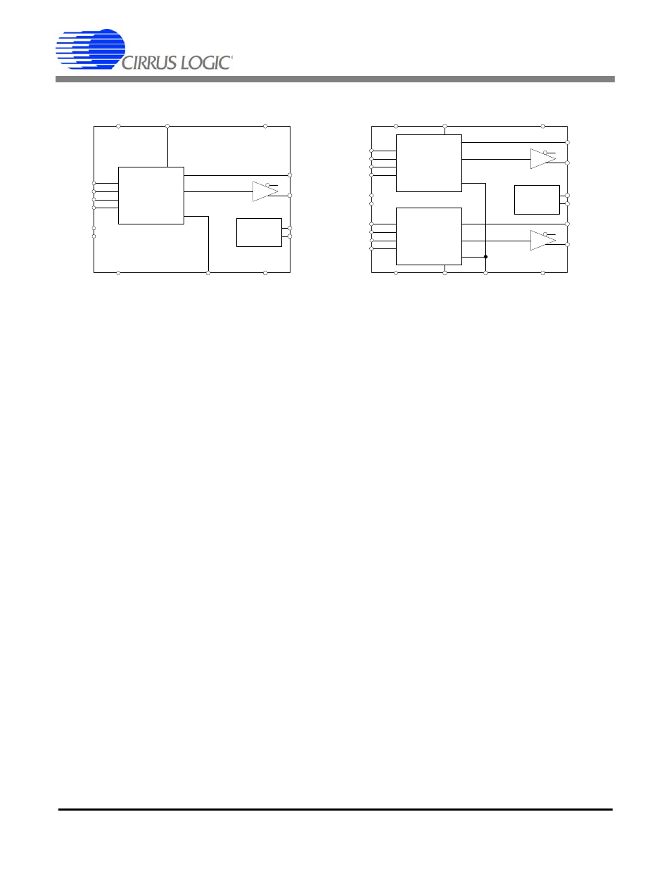
Modulator operation, 1 one’s density, Figure 10. cs5371a and cs5372a block diagrams – Cirrus Logic CS5372A User Manual
Page 14

CS5371A CS5372A
14
DS748F3
3. MODULATOR OPERATION
The CS5371A and CS5372A are one- and
two-channel, fourth-order
ΔΣ modulators opti-
mized for extremely high-resolution measure-
ment of signals between DC and 2000 Hz.
When combined with CS3301A / CS3302A dif-
ferential amplifiers, the CS4373A test DAC
and CS5376A digital filter, a small, low-power,
self-testing, high-accuracy, multi-channel
measurement system results.
The CS5371A and CS5372A modulators have
high dynamic range and low total harmonic
distortion with very low power consumption
and are optimized for extremely high-resolu-
tion measurement of 5 V
p-p
or smaller differen-
tial signals. They convert analog input signals
from the CS3301A / CS3302A differential am-
plifiers to an oversampled serial bit stream at
512 kbits per second which is then passed to
the digital filter.
The companion CS5376A digital filter gener-
ates the clock and synchronization inputs for
the CS5371A / CS5372A modulators while re-
ceiving the one-bit data and over-range flag
outputs. The digital filter decimates the modu-
lator’s oversampled output bit stream to a
high-resolution, 24-bit output at the selected
output word rate.
3.1 One’s Density
In normal operation a differential analog input
signal is converted to an oversampled
ΔΣ seri-
al bit stream on the MDATA output, with a
one’s density proportional to the differential
amplitude of the analog input signal.
One’s density of the MDATA output is defined
as the ratio of ‘1’ bits to total bits in the serial
bit stream output, i.e. an 86% one’s density
has, on average, a ‘1’ value in 86 of every 100
output data bits. The MDATA output has a
nominal 50% one’s density for a mid-scale dif-
ferential input, approximately 86% one’s den-
sity for a positive full-scale input signal, and
approximately 14% one’s density for a nega-
tive full-scale input signal.
Clock
Generator
INF1+
VREF+
VREF-
VA+
VA-
VD
GND
PWDN1
MFLAG1
MDATA1
MCLK
MSYNC
MFLAG2
MDATA2
PWDN2
INF1-
INR1-
INR1+
INF2+
INF2-
INR2-
INR2+
4th Order
ΔΣ Modulator
4th Order
ΔΣ Modulator
OFST
CS5372A
Clock
Generator
INF+
VREF+
VREF-
VA+
VA-
VD
GND
PWDN
MFLAG
MDATA
MCLK
MSYNC
INF-
INR-
INR+
4th Order
ΔΣ Modulator
OFST
CS5371A
Figure 10. CS5371A and CS5372A Block Diagrams
