Cirrus Logic CS5372A User Manual
Low-power, high-performance, Modulators, Features
Copyright
Cirrus Logic, Inc. 2010
(All Rights Reserved)
CS5371A
CS5372A
Low-power, High-performance
ΔΣ
Modulators
Features
Fourth-order
ΔΣ Architecture
Clock-jitter-tolerant Architecture
Input Voltage: 5 V
pp
Fully Differential
Input Signal Bandwidth: DC to 2 kHz
High Dynamic Range
• 127 dB SNR @ 215 Hz BW (2 ms sampling)
• 124 dB SNR @ 430 Hz BW (1 ms sampling)
Low Total Harmonic Distortion
• -118 dB THD typical (0.000126%)
Low Power Consumption
• Normal operation: 25 mW per channel
• Power down: 10 µW per channel
Small Footprint, 24-pin SSOP package
Multi-channel System Support
• 1-channel System: CS5371A
• 2-channel System: CS5372A
• 3-channel System: CS5371A + CS5372A
• 4-channel System: CS5372A + CS5372A
Bipolar Power Supply Configuration
• VA+ = +2.5 V; VA- = -2.5 V; VD = +3.3 V
Description
The CS5371A and CS5372A are one- and two-channel,
high-dynamic-range, fourth-order
ΔΣ modulators intend-
ed for geophysical and sonar applications. When
combined with CS3301A / CS3302A differential amplifi-
ers, the CS4373A test DAC and CS5376A digital filter, a
small, low-power, self-testing, high-accuracy, multi-
channel measurement system results.
The modulators have high dynamic range and low total
harmonic distortion with very low power consumption.
They convert differential analog input signals from the
CS3301A / CS3302A amplifiers to an oversampled seri-
al bit stream at 512 kbits per second. This oversampled
bit stream is then decimated by the CS5376A digital filter
to a 24-bit output at the selected output word rate.
In normal operation, power consumption is 5 mA per
channel. Each modulator can be independently powered
down to 500 µA per channel, and by halting the input
clock they will enter a micro-power state using only 2 µA
per channel.
The CS5371A and CS5372A modulators are available in
small 24-pin SSOP packages, providing exceptional per-
formance in a very small footprint.
ORDERING INFORMATION
See
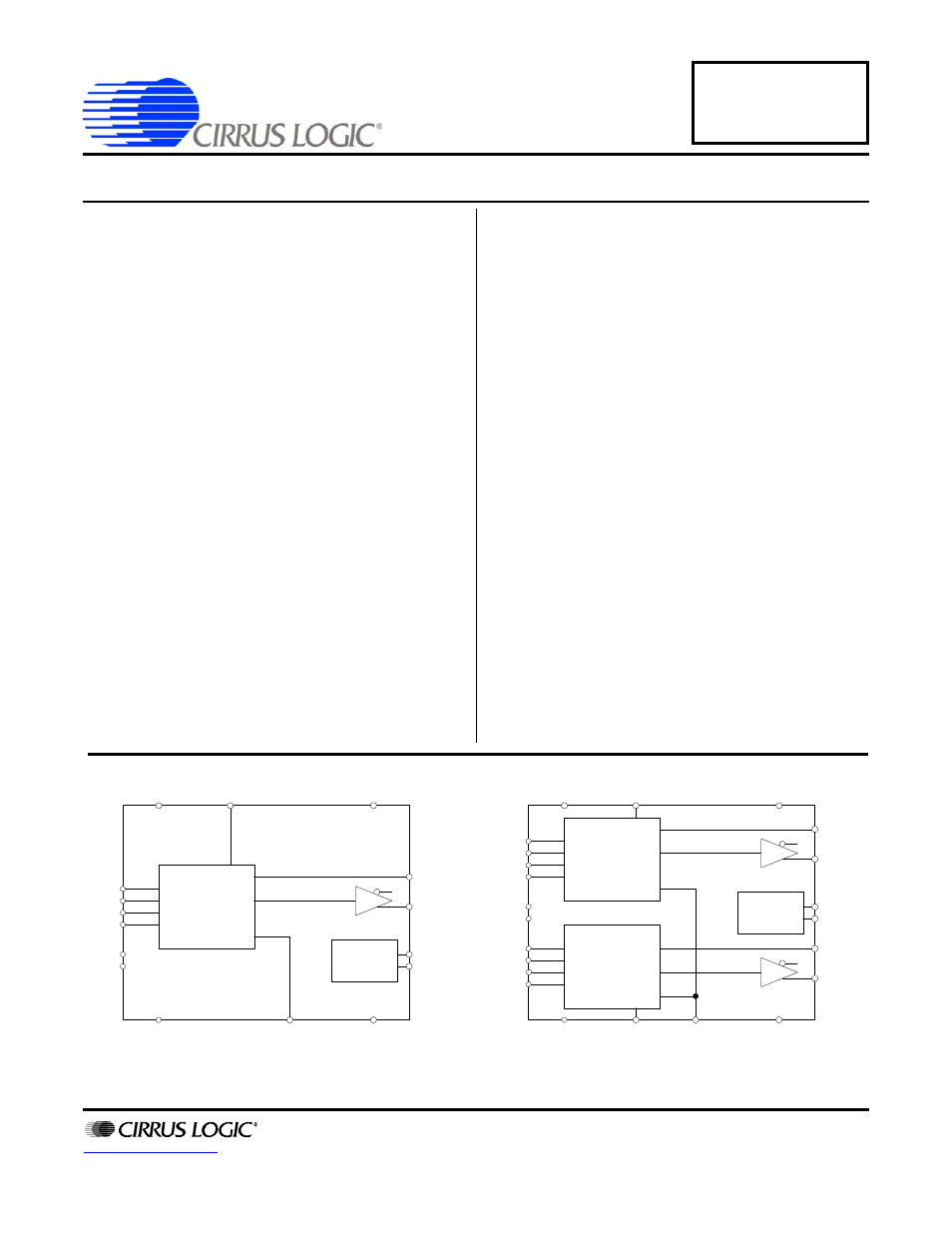
Clock
Generator
INF1+
VREF+
VREF-
VA+
VA-
VD
GND
PWDN1
MFLAG1
MDATA1
MCLK
MSYNC
MFLAG2
MDATA2
PWDN2
INF1-
INR1-
INR1+
INF2+
INF2-
INR2-
INR2+
4th Order
ΔΣ Modulator
4th Order
ΔΣ Modulator
OFST
CS5372A
Clock
Generator
INF+
VREF+
VREF-
VA+
VA-
VD
GND
PWDN
MFLAG
MDATA
MCLK
MSYNC
INF-
INR-
INR+
4th Order
ΔΣ Modulator
OFST
CS5371A
SEP ‘10
DS748F3
Document Outline
- Description
- Table of Contents
- List of Figures
- List of Tables
- 1. Characteristics and Specifications
- 2. System Diagram
- 3. Modulator Operation
- 4. Analog signals
- 5. Digital Signals
- 6. Power Modes
- 7. Voltage Reference
- 8. Power Supplies
- 9. Pin Description - CS5371A
- 10. Pin Description - CS5372A
- 11. Package Dimensions
- 12. Ordering Information
- 13. Environmental, Manufacturing, & Handling Information
- 14. Revision History