Appendix d cdb49x rev. a rework for i – Cirrus Logic CK4970x4 User Manual
Page 62
D-1
Copyright 2012 Cirrus Logic, Inc.
DS898CK7
Modifications to Improve the Signal Integrity of Debugger Communications
CK49x User’s Manual
Appendix D
CDB49x Rev. A Rework for I
2
C Buffer on DBCK Signal
D.1 Modifications to Improve the Signal Integrity of Debugger
Communications
The rework instructions in this appendix apply only to Rev. A of the CDB49x, and it is only necessary for
use of the proprietary debug port connected to the DSP. Normal demonstration features are not affected
by this modification.
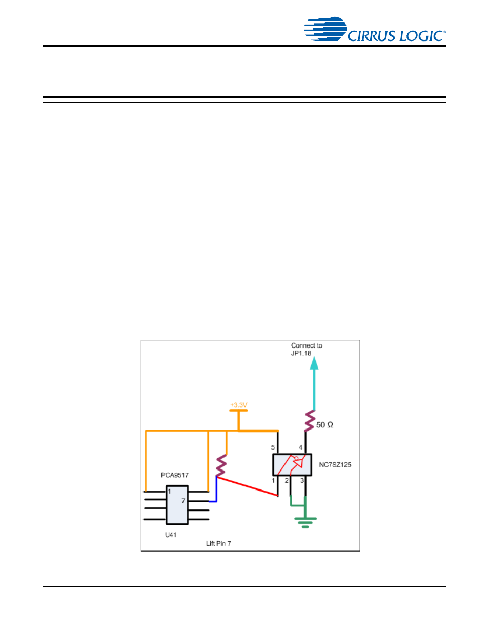
In order to improve the signal integrity of I
2
C communications, a modification has been created to buffer
the DBCK signal driven from the PCA9517 buffer and make its falling edge cleaner at the DSP.
1. Lift Pin 47 of U41.
2. Connect Pin 5 of the NC7SZ125 buffer to 3.3V.
3. Connect Pin 7 of U41 to Pin 1 of the NC7SZ125 buffer.
4. Connect a 3.3k resistor between Pins 1 and 5 of the NC7SZ125 buffer.
5. Connect Pins 2 and 3 of the NC7SZ125 buffer to GND on JP1.19 or JP1.20
6. Wire Pin 4 of the NC7SZ125 buffer to a 50
resistor, and connect the other end of the resistor to
JP1.18
shows the logical representation of the modifications
Figure D-1. Logical Representation of Appendix D Modifications.