2 clock and data flow for s/pdif input, 2 clock and data flow for s/pdif input -12, Figure 1-6. cs495xxx/cs497xxx s/pdif clocking -12 – Cirrus Logic CK4970x4 User Manual
Page 19: Table 1-3. s/pdif clocking -12
CK49x System Description
CK49x User’s Manual
DS898CK7
Copyright 2012 Cirrus Logic, Inc
1-12
Note:
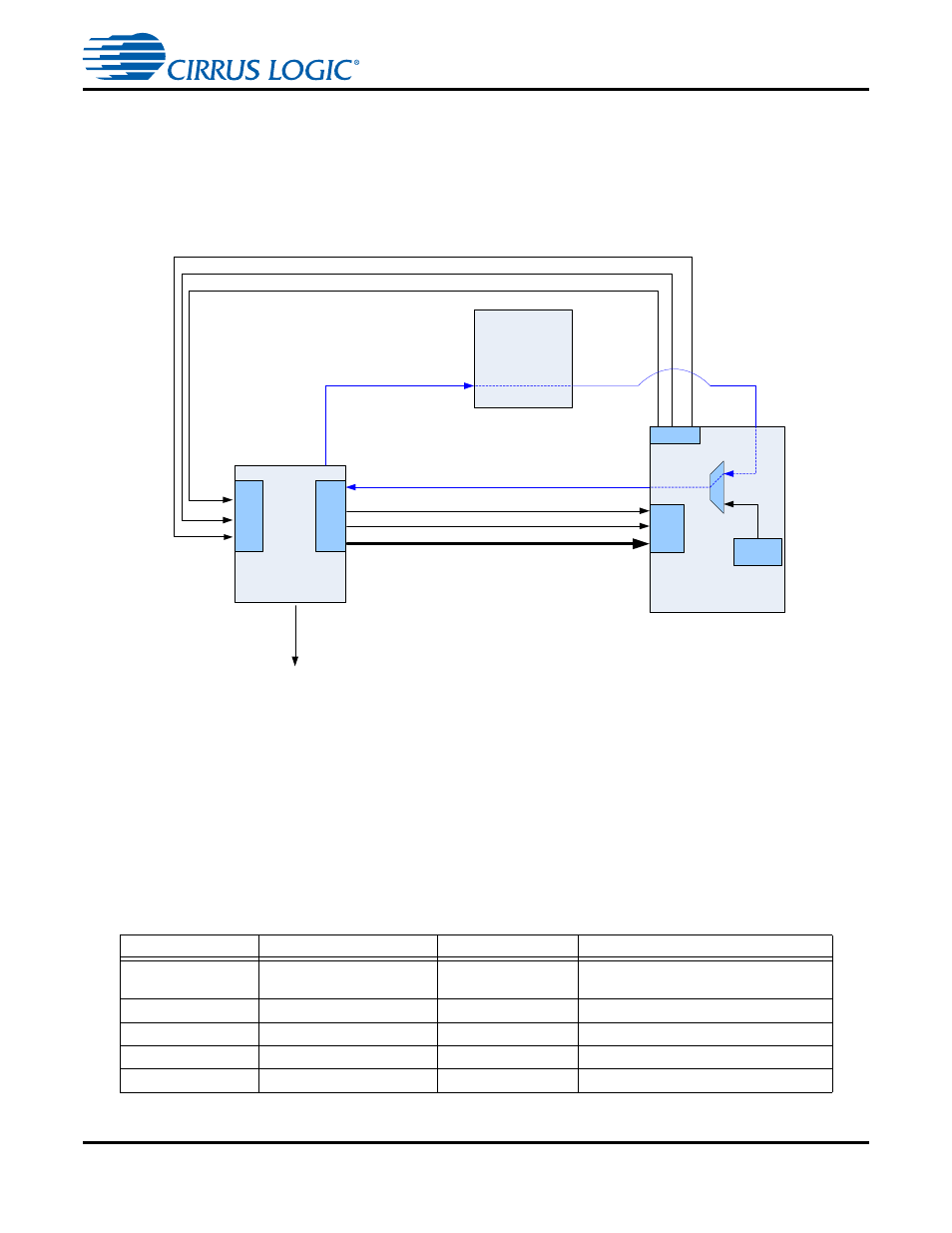
MUXED_MCLK is the clock signal that is driven by the CS42528’s RMCK pin. The CS42528
provides the recovered clock from the S/PDIF input unless it loses signal lock, in which case the
CS42528 passes the DSP clock (XTAL_OUT) that it receives on the OMCK pin via the CS2000.
1.3.20.2 Clock and Data Flow for S/PDIF Input
Figure 1-6. CS495xxx/CS497xxx S/PDIF Clocking
The S/PDIF clocking architecture is used when any S/PDIF RX is used as an audio source. That is, any S/
PDIF RX is selected, and the audio input source multiplexer (U23) is used to select CODEC audio
sources.
illustrates this clocking configuration.
MCLK recovered from the incoming S/PDIF stream must be MCLK for the system, and the codec masters
the input clocks (CODEC_SCLK/CODEC_LRCLK) of the CS495xxx/CS497xxx. In this configuration the
internal multiplexer of the CS42528 routes the recovered MCLK to MUXED_MCLK.
The CS495xxx/CS497xxx always masters its output clocks (OUT_DAO1_SCLK/OUT_DAO1_LRCLK).
Note:
MUXED_MCLK is the clock signal that is driven by the CS42528’s RMCK pin. The CS42528
Table 1-3. S/PDIF Clocking
Clock Name
Clock Master Source
Clock Driver
Clock Frequency
MUXED_MCLK
CS42528
CS42528
512*S/PDIF Fs
(e.g. 24.576 MHz for 48 kHz),
CODEC_SCLK
MUXED_MCLK
CS42528
64*Input Fs (default)
CODEC_LRCLK
MUXED_MCLK
CS42528
Input Fs
OUT_DAO1_SCLK
MUXED_MCLK
CS495xxx/CS497xxx
64*Output Fs (default)
OUT_DAO1_LRCLK
MUXED_MCLK
CS495xxx/CS497xxx
1*Input Fs (default)
OUT_DAO1_SCLK
OUT_DAO1_LRCLK
OUT_DA01_D[3:0]
XM
TA
S/
PDIF
OUT
MUXED_BUF_MCLK
DAI
DAO
SDIN
CS42528
XT
AL_
O
UT
CS2000
S/PDIF
RX
CODEC_SCLK
CODEC_LRCLK
CODEC_DOUT
SDOUT
CS4953x
DSP-1