1 clock and data flow for adc input, 1 clock and data flow for adc input -11, Figure 1-5. cs495xxx/cs497xxx adc clocking -11 – Cirrus Logic CK4970x4 User Manual
Page 18: Table 1-2. adc clocking -11, Cs2000
1-11
Copyright 2012 Cirrus Logic, Inc.
DS898CK7
CK49x System Description
CK49x User’s Manual
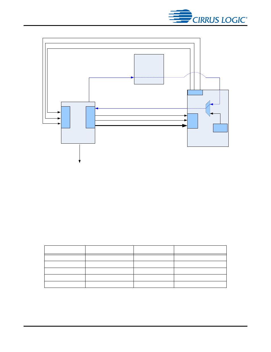
1.3.20.1 Clock and Data Flow for ADC Input
Figure 1-5. CS495xxx/CS497xxx ADC Clocking
The ADC clocking architecture is used when the ADCs are used as the only audio input (i.e. S/PDIF is
disabled, and the audio input source multiplexer (U23) is used to select CODEC audio sources.
illustrates this clocking configuration.
XTAL_OUT from the CS495xxx/CS497xxx is MCLK for the system via the CS2000 and CS42528 clocking
mux, and the codec masters the input clocks (MUXED_SCLK/MUXED_LRCLK) of the CS495xxx/
CS497xxx. The system routing of the clocks was simplified by using the CS42528 to drive MCLK to the
system, but the internal clock multiplexer of the CS42528 is forced to the OMCK setting to pass
XTAL_OUT.
The CS495xxx/CS497xxx always masters its output clocks (OUT_DAO1_SCLK/OUT_DAO1_LRCLK).
Table 1-2. ADC Clocking
Clock Name
Clock Master Source
Clock Driver
Clock Frequency
MUXED_BUF_MCLK
CS495xxx/CS497xxx
CS42528
24.576 MHz
CODEC_SCLK
MUXED_BUF_MCLK
CS42528
64*Input Fs (default)
CODEC_LRCLK
MUXED_BUF_MCLK
CS42528
Input Fs
OUT_DAO1_SCLK
MUXED_BUF_MCLK
CS495xxx/CS497xxx
64*Output Fs (default)
OUT_DAO1_LRCLK
MUXED_BUF_MCLK
CS495xxx/CS497xxx
1*Input Fs (default)
OUT_DAO1_SCLK
OUT_DAO1_LRCLK
OUT_DA01_D[3:0]
XMT
A
S
/PD
IF
OUT
MUXED_BUF_MCLK
DAI
DAO
SDIN
CS42528
XT
A
L_O
U
T
CS2000
S/PDIF
RX
CODEC_SCLK
CODEC_LRCLK
CODEC_DOUT
SDOUT
CS4953x
DSP-1