2 ground, 3 decoupling, 2 pll filter – Cirrus Logic CS485xx User Manual
Page 91: 1 analog power conditioning
9-11
Copyright 2009 Cirrus Logic, Inc.
DS734UM7
Pin Description
CS485xx Hardware User’s Manual
9.2.1.2 Ground
For two-layer circuit boards, care should be taken to have sufficient grounding between the DSP and parts in
which it will be interfacing (DACs, ADCs, S/PDIF Receivers, microcontrollers, and especially external
memory). Insufficient grounding can degrade noise margins between devices resulting in data integrity
problems.
9.2.1.3 Decoupling
It is necessary to decouple the power supply by placing capacitors directly between the power and ground of
the CS485xx. Each pair of power/ground pins (VDD1/GND1, etc.) should have its own decoupling capacitor.
The recommended procedure is to place a 0.1 uF capacitor as close as physically possible to each power
pin connected with a wide, low-inductance trace. A bulk capacitor of at least 10 uF is recommended for each
power plane.
9.2.2 PLL Filter
9.2.2.1 Analog Power Conditioning
In order to obtain the best performance from the CS485xx internal PLL, the analog power supply VDDA
must be as noise free as possible. A ferrite bead and two capacitors should be used to filter the VDDIO to
generate VDDA. This power scheme is shown in the Typical Connection diagrams.
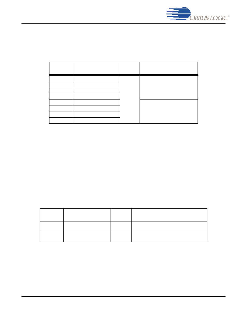
Table 9-3. Core and I/O Ground Pins
LQFP-48
Pin #
Pin Name
Pin Type
Pin Description
4
GND1
Input
Core Ground.
9
GND2
22
GND3
33
GND4
7
GNDIO1
I/O Ground
19
GNDIO2
30
GNDIO3
40
GNDIO4
Table 9-4. PLL Supply Pins
LQFP-48
Pin #
Pin Name
Pin Type
Pin Description
48
VDDA
Input
PLL supply. This voltage must be 3.3V. This
must be clean, noise-free analog power.
46
GNDA
Input
PLL ground. This ground should be as noise-
free as possible.