Chapter 7: crystal oscillator and system clocking, 1 system clocking controls – Cirrus Logic CS485xx User Manual
Page 77
7-1
Copyright 2008 Cirrus Logic, Inc.
DS734UM7
System Clocking Controls
CS485xx Hardware User’s Manual
Chapter 7
Crystal Oscillator and System Clocking
7.1 System Clocking Controls
The CS485xx incorporates one programmable phase locked loop (PLL) clock synthesizer. The PLL take an
input reference clock and produces all the clocks required to run the DSP and peripherals.
The input reference clock may come from an external 24.576 MHz oscillator connected to the XTI pin. In this
case the XTO pin should be left disconnected. This is the preferred source in A/V Receiver designs that
require low-jitter clocks.
The built in crystal oscillator circuit may be used to generate the reference clock for the PLLs. A parallel
resonant-type crystal is connected between the XTI and XTO pins as shown in
Figure 7-1
. The value of C1
is specific to each crystal. The CS485xx Data Sheet specifies acceptable crystal parameters (including C
L
and ESR).
When a crystal is used, XTAL_OUT may be used to clock other devices in the system such as an external S/
PDIF receiver.
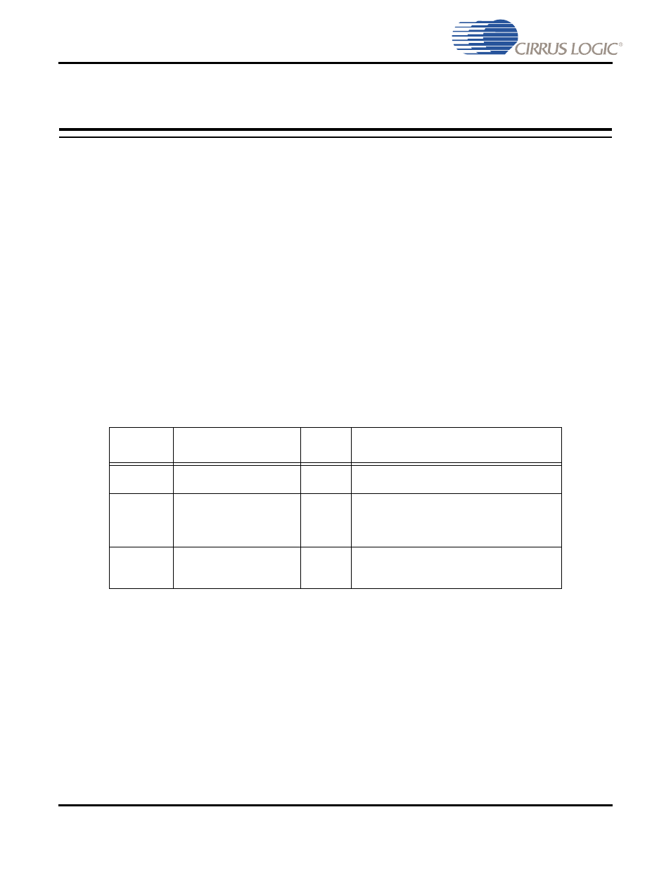
Table 7-1
describes the XTAL_OUT, XTI, and XTO pins.
The PLL is controlled by the clock manager in the DSP O/S application software. AN298, CS485xx Firmware
User’s Manual should be referenced regarding what CLKIN input frequency and PLL multiplier values are
supported.
Figure 7-1
shows the schematic of the CS485xx crystal oscillator.
Table 7-1. DSP Core Clock Pins
LQFP-100
Pin #
Pin Name
Pin
Type
Pin Description
43
XTAL_OUT
Output
Buffered version of XTI. Can be programmed
to be Fxtal / 2.
44
XTI
Input
Reference Clock Input/Crystal Oscillator Input.
An external clock may be input directly to this
pin or one end of a crystal may be connected
to this pin.
45
XTO
Output
Crystal Oscillator Output. One end of a crystal
oscillator is connected to this pin. This pin
cannot be used to drive external circuitry.