Cdb47xxxs, Use daughtercard – Cirrus Logic CDB470xx User Manual
Page 55

DS886
DB11
Co
pyrigh
t 201
4 Cirrus Log
ic, Inc
6
-4
CDB47xxS Singl
e-Ende
d Sch
e
matic
D
e
scription
s
CDB47xxx User’s Manual
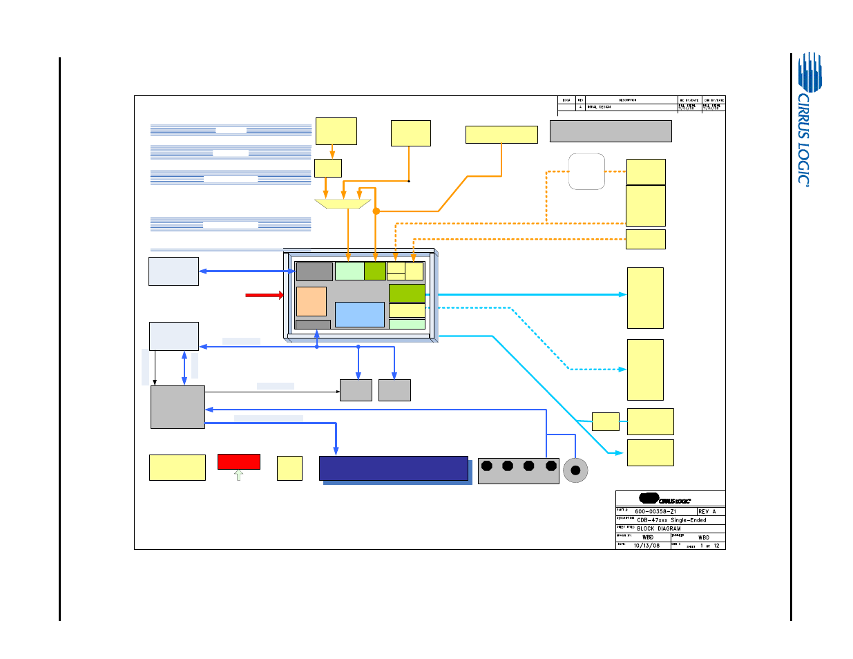
Figure 6-1. CDB47xxxS (Sngle-ended) Board Block Diagram
CS47xxx
I2S IN HDR
I2S OUT
HDR
(8 ch)
8ch
RCA
OUT
Power In
20 Pin HDR
Standard 20 Pin Debug Header (Serial Control & Debug)
SPI
FLASH
USB MCU
Silicon Labs
SPDIF - OUT
OPTICAL
SMALL
20-PIN HDR
I2S HDRs
Header will be available to probe / bring in I2S signals
SPI_HOLD
Control
Co
n
tro
l
EX
T CTRL
SE
L
Power
LEDs
5:1
mux
ADC
SPDIF
Rx
SPDIF Tx
DAC
I2S in
(8 ch)
I2S out
(8 ch)
Control
USB
(DSP
Composer)
CDB47XXXS
Analog
Analog
Digital
Digital
Digital
DSP CORE
Digital
Use
DaughterCard
SRC
ADC
LCD Panel
Control (Parallel Port)
B1 B2 B3 B4
Buttons
Rotary Knob
GPIO
Mic Input
Jack
Mic
Pre-Amp
Circuitry
RCA
IN
2 ch (x4)
RCA IN
2ch
GPIO
GPIO
HDR
Wall Adapter
DSP Daughtercard
The Chronos DSP Daughercard will have only the DSP.
This allows us to easily swap out the DSP for different
CS47xxx Family members.
DAO Buttons/LEDs
DAO pins on Chronos are also GPIO. These buttons/LEDs
Can be used by the new primitives being developed
SPDIF - IN
COAX
Buffer
SPDIF - IN
OPTICAL
Buffer
SPDIF - OUT
COAX
I2C
FLASH
