21xx core – Analog Devices ADSP-2181 User Manual
Page 3
ADSP-2181/ADSP-2183
REV. 0
–3–
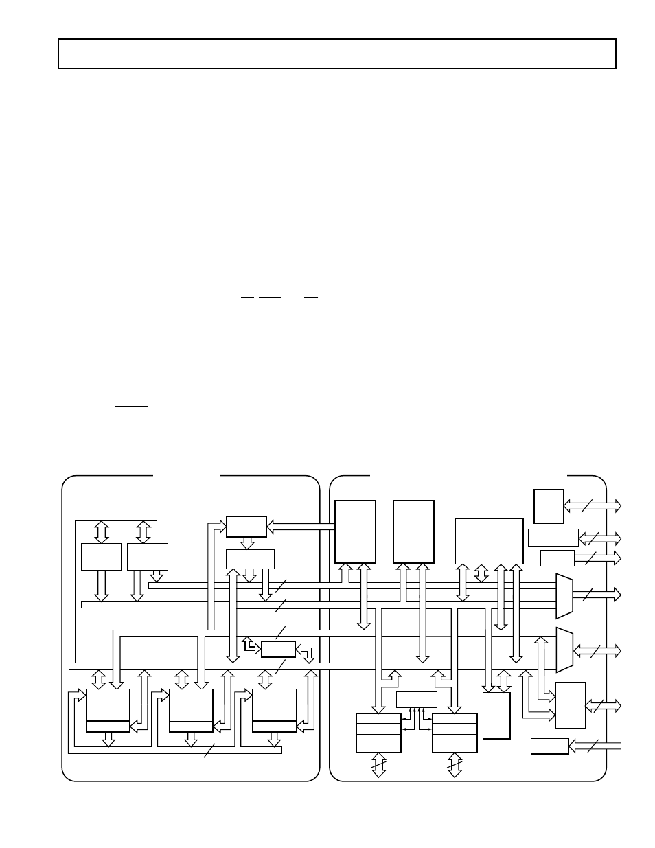
Program memory can store both instructions and data, permit-
ting the ADSP-2181/ADSP-2183 to fetch two operands in a
single cycle, one from program memory and one from data
memory. The ADSP-2181/ADSP-2183 can fetch an operand from
program memory and the next instruction in the same cycle.
In addition to the address and data bus for external memory
connection, the ADSP-2181/ADSP-2183 has a 16-bit Internal
DMA port (IDMA port) for connection to external systems.
The IDMA port is made up of 16 data/address pins and five
control pins. The IDMA port provides transparent, direct access
to the DSPs on-chip program and data RAM.
An interface to low cost byte-wide memory is provided by the
Byte DMA port (BDMA port). The BDMA port is bidirectional
and can directly address up to four megabytes of external RAM
or ROM for off-chip storage of program overlays or data tables.
The byte memory and I/O memory space interface supports slow
memories and I/O memory-mapped peripherals with program-
mable wait state generation. External devices can gain control of
external buses with bus request/grant signals (BR, BGH, and BG).
One execution mode (Go Mode) allows the ADSP-2181/ADSP-
2183 to continue running from on-chip memory. Normal execu-
tion mode requires the processor to halt while buses are granted.
The ADSP-2181/ADSP-2183 can respond to eleven interrupts.
There can be up to six external interrupts (one edge-sensitive,
two level-sensitive, and three configurable) and seven internal
interrupts generated by the timer, the serial ports (SPORTs),
the Byte DMA port, and the power-down circuitry. There is
also a master RESET signal.
The two serial ports provide a complete synchronous serial inter-
face with optional companding in hardware and a wide variety of
framed or frameless data transmit and receive modes of operation.
Each port can generate an internal programmable serial clock or
accept an external serial clock.
The ADSP-2181/ADSP-2183 provides up to 13 general-purpose
flag pins. The data input and output pins on SPORT1 can be
alternatively configured as an input flag and an output flag. In
addition, there are eight flags that are programmable as inputs
or outputs, and three flags that are always outputs.
A programmable interval timer generates periodic interrupts. A
16-bit count register (TCOUNT) is decremented every n pro-
cessor cycles, where n is a scaling value stored in an 8-bit regis-
ter (TSCALE). When the value of the count register reaches
zero, an interrupt is generated and the count register is reloaded
from a 16-bit period register (TPERIOD).
Serial Ports
The ADSP-2181/ADSP-2183 incorporates two complete syn-
chronous serial ports (SPORT0 and SPORT1) for serial com-
munications and multiprocessor communication.
Here is a brief list of the capabilities of the ADSP-2181/ADSP-
2183 SPORTs. Refer to the ADSP-2100 Family User’s Manual
for further details.
• SPORTs are bidirectional and have a separate, double-
buffered transmit and receive section.
• SPORTs can use an external serial clock or generate their
own serial clock internally.
• SPORTs have independent framing for the receive and trans-
mit sections. Sections run in a frameless mode or with frame
synchronization signals internally or externally generated.
Frame sync signals are active high or inverted, with either of
two pulse widths and timings.
OUTPUT REGS
ALU
OUTPUT REGS
MAC
5
TIMER
INPUT REGS
INPUT REGS
DATA
ADDRESS
GENERATOR
#1
DATA
ADDRESS
GENERATOR
#2
21xx CORE
PMA BUS
DMA BUS
PMD BUS
INSTRUCTION
REGISTER
PROGRAM
SEQUENCER
BUS
EXCHANGE
DMD BUS
PROGRAM
SRAM
16k
×
24
DATA
SRAM
16k
×
16
BYTE
DMA
CONTROLLER
MUX
14
14
24
16
DMD
BUS
PMA BUS
DMA BUS
PMD BUS
INPUT REGS
SHIFTER
OUTPUT REGS
INPUT REGS
MAC
OUTPUT REGS
INPUT REGS
ALU
OUTPUT REGS
R BUS
16
TRANSMIT REG
RECEIVE REG
SERIAL
PORT 0
TRANSMIT REG
RECEIVE REG
SERIAL
PORT 0
COMPANDING
CIRCUITRY
5
5
INTERNAL
DMA
PORT
INTERRUPTS
POWER
DOWN
CONTROL
LOGIC
2
8
3
MUX
PROGRAMMABLE
I/O
FLAGS
14
EXTERNAL
ADDRESS
BUS
EXTERNAL
DATA
BUS
16
4
24
ADSP-2181/ADSP-2183 INTEGRATION
Figure 1. ADSP-2181/ADSP-2183 Block Diagram