Atec Aeroflex-IFR-3416 User Manual
Page 9
Interpolation Factor
Automatically selected
Reconstruction Filter Stop Band Attenuation
> 70 dB
ARB Spectral Purity
Spurious free dynamic range > 70 dB, typically > 80 dB
20 kHz offset phase noise
< -120 dBc/Hz
Floor noise
< -140 dBc/Hz
ation, formatting and downloading of ARB waveform files to the 3410
series.
A waveform library is provided on a CD containing a selection of files
for testing 2G, 2.5G and 3G systems. Files can be downloaded from
Marker Control Bits
Up to 3 marker bits (1-3) can be attached to each sample of IQ data.
These can be used to indicate significant points in the waveform and
are available as HC CMOS outputs via the rear panel Aux IN/OUT con-
nector. Marker bit 1 can be used as RF Burst Control signal. Marker
bit 2 can be used as Burst Attenuation Trigger signal to decrease
(attenuate) the RF level from its nominal value.
Control Mode
Continuous, single or triggered operation of the ARB
An external TTL trigger input signal is available on the AUX IN/OUT rear
panel connector.
IQ Outputs (Not applicable with Option 009 fitted)
The IQ signals produced by the ARB are available on the rear panel
I/AM OUT and Q/FM OUT BNC connectors. Output level is 0.5 V RMS
EMF (vector sum) from a source impedance of 50 .
Allows the creation of digitally modulated signals using generic modula-
tion formats. An internal data source provides PRBS or fixed patterns.
External real-time data in the form of symbol data, or digital IQ data
may be applied via an LVDS interface.
Generic Modulation Formats
PSK
BPSK, QPSK, 8PSK, 16PSK
8PSK EDGE (8PSK with 3 /8 rotation)
/2 DBPSK, /4 DQPSK, /8 D8PSK
DBPSK, DQPSK, D8PSK
OQPSK (time offset)
MSK
GMSK
FSK/GFSK
2 and 4 level symmetric
QAM
16, 32, 64, 128, 256 levels
For data bit to symbol mapping information refer to Technical Note
"IFR 3410 Option 8 RTBB Ancillary Information"
SYMBOL RATE
Range
5 kHz to 2 MHz. Resolution 1 Hz
BASEBAND CHANNEL FILTERS
Filter Types
Nyquist
a = 0.1 to 0.8, resolution 0.01
Root Nyquist
a = 0.1 to 0.8, resolution 0.01
Gaussian
Bt 0.1 to 1.0, resolution 0.1
EDGE
"Linearized Gaussian" as defined in GSM 05.04
DATA SOURCE
Formats
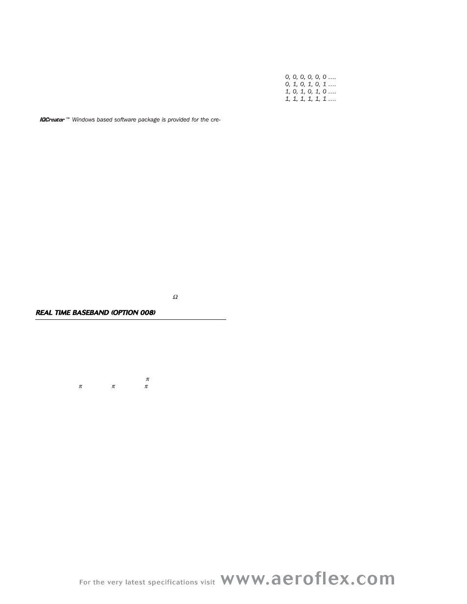
Internal Data PRBS - PN9, PN11, PN15, PN16, PN20, PN21, PN23.
Fixed Pattern consisting of -
User-defined symbol file stored in non-volatile memory
(Max size 256 kB)
External Serial Data
A single bit stream representing symbol information can be applied.
The bit to symbol conversion is determined from the selected modula-
tion type.
External Parallel Data
Symbol information consisting of 1 to 8 data bits can be applied.
External parallel and serial data is input via the LVDS connector on the
rear panel.
DATA ENCODING
None, Differential, GSM Differential, Inverted
TIMING/SYNCHRONIZATION
All clock and synchronization signals are provided internally by Option 8
RTBB and made available to the user on the rear panel LVDS connec-
tor. An external clock may be phase aligned to the internal clock via a
"sync" operation.
External Serial Data Clock
Eight times the symbol rate, for all modulation types.
External Parallel Data Clock
Nominal symbol rate
FREQUENCY HOPPING
Frequency Hop List
Up to 32 frequency values. The frequency values entered represent
offset values from the current RF frequency.
Frequency Offset Values
Offset values range ± 10 MHz
MODES
Linear
On receipt of a hop trigger, the next frequency in the list is indexed.
Random
On receipt of a hop trigger, an internal PRBS generator indexes
through the frequency list. PN length and polynomial initial seed value
are user selectable. PN values selectable from - 9, 11, 15, 16, 20,
21, and 23.
External
On receipt of a hop trigger, the 5-bit hop address lines applied to the
LVDS connector are used to index the frequency list.
Hop Rate
Max hop rate (hops/sec) is half symbol rate. Hopping is synchronized
to symbol transition.
DIGITAL IQ DATA
Digital IQ data is available via the LVDS connector on the rear panel.
EXTERNAL IQ DATA IN
External 16-bit IQ data can be applied to an LVDS interface. The data
can then be filtered or not, depending on the application, by the base-
band board and fed to the DACs. All clock and sync signals are located