Atec Aeroflex-IFR-3416 User Manual
Page 7
Accuracy
At 1 kHz rate
± 4% of set depth ± 1% excluding residual AM
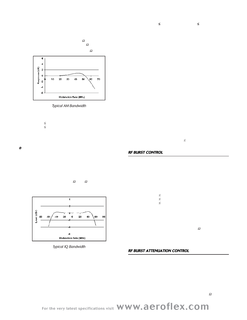
AM Bandwidth
1 dB
DC to 200 kHz (DC coupled, 100 k )
10 Hz to 200 kHz (AC coupled, 100 k )
3 dB
Typically 30 MHz (DC or AC coupled, 50 )
Total Harmonic Distortion
For 1 kHz modulation rate
< 1% for depths 30%
< 2% for depths 80%
FM on AM
Typically < 20 Hz for 30% AM depth at a modulation rate of 1 kHz and
carrier frequency of 500 MHz
M on AM
Typically < 0.02 radian for 30% AM depth at a modulation rate of
1 kHz and carrier frequency of 500 MHz
IQ MODULATION
Performance applicable in ACP and Noise modes only
IQ Inputs
BNC connector inputs, selectable 50 /100 k
input impedance
Full scale input (I
2
+Q
2
)
0.5
occurs for 0.5 V rms (The level requested is
obtained by applying 0.5 VDC to either the I or Q input)
Modulation Bandwidth Relative to DC
At 23°C ± 5°C:
± 0.5 dB for frequencies DC up to 5 MHz
1 dB for frequencies DC up to 10 MHz
3 dB:
RF Mode
2.8 GHz
6 GHz
Noise
> 42 MHz, 50 MHz typ
> 35 MHz, 45 MHz typ
ACP
> 48 MHz, 55 MHz typ
> 40 MHz, 50 MHz typ
DC Vector Accuracy
Relative to Full Scale (0.5 V RMS)
Static Error Vector Magnitude (EVM)
< 1% RMS at full scale
Magnitude error
< 0.5% RMS at full scale
Phase error
< 0.5° RMS at full scale
Residual Carrier Magnitude:
For 0 V input voltage, relative to full scale
RF Mode
Noise
< -45 dBc, typically < -55 dBc
ACP
< -40 dBc, typically < -50 dBc
Valid for 12 hours after executing an IQ self-calibration and within
± 5°C of the calibration temperature. The instrument displays a warn-
ing if the time or temperature limits are exceeded.
Static EVM and phase error measured with residual carrier magnitude
removed.
IQ Image Suppression
At 10 kHz modulation frequency
Typically < -50 dBc @ 10 kHz
Linearity (See linearity chart over page)
Adjacent Channel Power (ACP), in ACP mode for continuous and dis-
continuous signals at RF output levels 0 dBm, over the temperature
range 23°C ± 5°C
A digital control bit is used to generate an analog ramp (up or down)
of the RF output. The Burst Gate control signal can either be generat-
ed internally as part of the optional internal base-band source, or pro-
vided externally by the user on the rear panel connector. When inter-
nally generated, the Burst Gate control signal appears on the rear
panel auxiliary connector that then serves as an output.
On/Off Ratio
For the temperature range 23°C ± 5°C
> 90 dB for carriers 3 GHz
> 80 dB for carriers 4 GHz
> 65 dB for carriers 6 GHz
Ramp Profile
Rise and fall time after the L-H and H-L transitions of the burst control
bit respectively can be defined by the user from 10 µs to 999 µs in
0.1 µs steps.
Burst Gate control input is a TTL level (HCT), 50
impedance BNC
input on the rear panel.
RF ramp can be adjusted in time by ± 50 µs in increments of
0.1 µs with respect to the trigger event.
A digital attenuation control bit (in conjunction with the ramp control
bit) is used to decrease the RF level from the set level to an alternative
level during burst modulation. The Burst Attenuation Trigger signal can
be provided internally as part of the optional dual arbitrary waveform
generator (ARB), or externally on a rear panel connector. When inter-
nally generated, the Burst Attenuation Trigger control signal appears on
the rear panel auxiliary connector that then serves as an output.
Attenuation range available is 0 to 70 dB.
Burst Attenuation Trigger control is a TTL level (HCT), 50
impedance