Data sheet, Feature descriptions (continued) – GE Industrial Solutions QBDW033A0B Barracuda Series User Manual
Page 10
GE
Data Sheet
QBDW033A0B Barracuda Series; DC-DC Converter Power Modules
36-75Vdc Input; 12.0Vdc, 33.0A, 400W Output
May 9, 2013
©2012 General Electric Company. All rights reserved.
Page 10
Feature Descriptions (continued)
Load Sharing
For higher power requirements, the QBDW033A0 power
module offers an optional feature for parallel operation (-P
Option code). This feature provides a precise forced output
voltage load regulation droop characteristic. The output set
point and droop slope are factory calibrated to insure
optimum matching of multiple modules’ load regulation
characteristics. To implement load sharing, the following
requirements should be followed:
The V
OUT
(+) and V
OUT
(-) pins of all parallel modules must be
connected together. Balance the trace resistance for each
module’s path to the output power planes, to insure best
load sharing and operating temperature balance.
V
IN
must remain between 40V
dc
and 75V
dc
for droop
sharing to be functional.
It is permissible to use a common Remote On/Off signal to
start all modules in parallel.
These modules contain means to block reverse current
flow upon start-up, when output voltage is present from
other parallel modules, thus eliminating the requirement
for external output ORing devices. Modules with the –P
option will self determine the presence of voltage on the
output from other operating modules, and automatically
increase its Turn On delay, T
delay
, as specified in the Feature
Specifications Table.
When parallel modules startup into a pre-biased output,
e.g. partially discharged output capacitance, the T
rise
is
automatically increased, as specified in the Feature
Specifications Table, to insure graceful startup.
Insure that the load is <50% I
O,MAX
(for a single module) until
all parallel modules have started (load full start > module
T
delay
time max + T
rise
time).
If fault tolerance is desired in parallel applications, output
ORing devices should be used to prevent a single module
failure from collapsing the load bus.
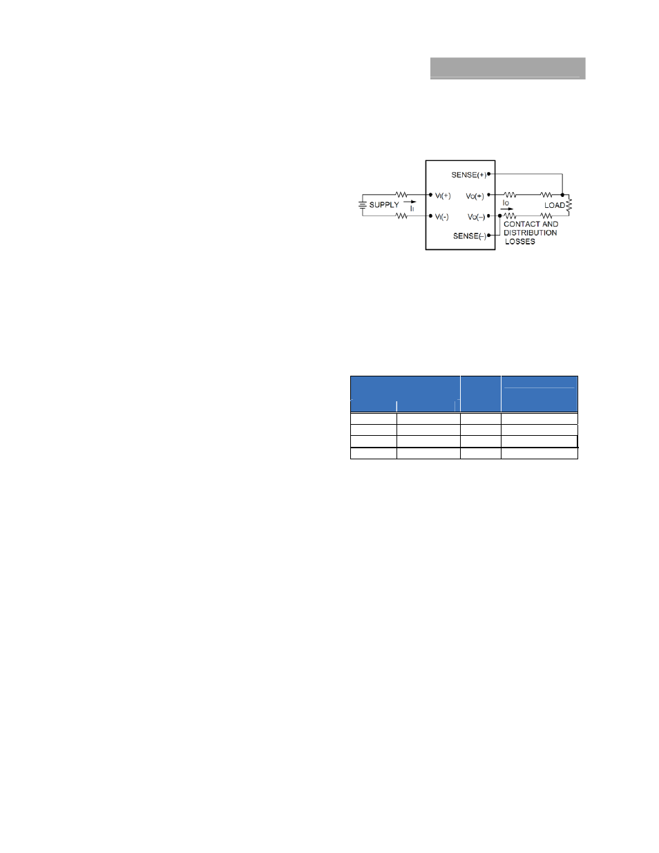
Remote Sense
Remote sense minimizes the effects of distribution losses by
regulating the voltage at the remote-sense connections (See
Figure 15). The SENSE(-) pin should be always connected to
VO(–).The voltage between the remote-sense pins and the
output terminals must not exceed the output voltage sense
range given in the Feature Specifications table:
[V
O
(+) – V
O
(–)] – [SENSE(+) ] 0.5 V
Although the output voltage can be increased by both the
remote sense and by the trim, the maximum increase for
the output voltage is not the sum of both. The maximum
increase is the larger of either the remote sense or the trim.
The amount of power delivered by the module is defined as
the voltage at the output terminals multiplied by the output
current. When using remote sense and trim, the output
voltage of the module can be increased, which at the same
output current, would increase the power output of the
module. Care should be taken to ensure that the maximum
output power of the module remains at or below the
maximum rated power (Maximum rated power = Vo,set x
Io,max).
Figure 15. Circuit Configuration for remote sense.
Configurable Control Pins
The QBDW033A0B contains two configurable control pins,
T/C1 and C2, referenced to the module secondary SIG_GND.
See Mechanical Views for pin locations. The following table
list the default factory configurations for the functions
assigned to these pins. Additional configurations can be
accomplished via the PMBus command,
MFR_CPIN_ARA_CONFIG. Following the table, there is a
feature description for each function.
Pin
Designation/Function Module
Code
Configuration
T/C1
C2
On/Off (O) Power Good
w/o -P
Factory Default
Trim
On/Off (O)
w/o -P
Via PMBus
Trim
Power Good
w/o -P
Via PMBus
On/Off (O) Power Good
with -P
Factory Default
Remote On/Off(o)
The module contains an additional remote on/off control
input On/Off(o), via either the T/C1 or C2 pin, reference to the
V
O
(-) terminal. The factory default configuration is set to
ignore this input, unless activated by the PMBus command,
MFR_ CPIN_ON_OFF_CONFIG. This command is also used to
configure the logic for the On/Off(o) pin. Positive logic
remote on/off turns the module on during a logic-high
voltage on the ON/OFF pin, and off during a logic low.
Negative logic remote on/off turns the module off during a
logic high, and on during a logic low. The On/Off(o) circuit is
powered from an internal bias supply, referenced to
SIG_GND. To turn the power module on and off, the user
must supply a switch to control the voltage between the
On/Off (o) terminal and the V
O
(-) terminal (V
on/off
(o)). The
switch can be an open collector or equivalent (see Figure
13). A logic low is V
on/off
(o)
= -0.3V to 0.8V. The typical I
on/off
(o)
during a logic low is 330µA. The switch should maintain a
logic-low voltage while sinking 250µA. During a logic high,
the maximum V
on/off
(o)
generated by the power module is
3.3V. The maximum allowable leakage current of the switch
at V
on/off
(o) = 2.0V is 130µA. If using an external voltage
source, the maximum voltage V
on/off
on the pin is 3.3V with
respect to the V
i
(-) terminal.
If not using the Remote On/Off(o) feature, the pin may be
left N/C
.