Ge energy, 2a dlynx, Non-isolated dc-dc power modules – GE Industrial Solutions 2A DLynx User Manual
Page 12: Datasheet, Test configurations, Design considerations, Input filtering
GE Energy
Datasheet
2A DLynx
TM
: Non-Isolated DC-DC Power Modules
3Vdc –14Vdc input; 0.6Vdc to 5.5Vdc output; 2A Output Current
June 24, 2013
©2012 General Electric Company. All rights reserved.
Page 12
Test Configurations
TO OSCILLOSCOPE
CURRENT PROBE
L
TEST
1μH
B
A
TTE
R
Y
C
S
1000μF
Electrolytic
E.S.R.<0.1
Ω
@ 20°C 100kHz
2x100μF
Tantalum
V
IN
(+)
COM
NOTE: Measure input reflected ripple current with a simulated
source inductance (L
TEST
) of 1μH. Capacitor C
S
offsets
possible battery impedance. Measure current as shown
above.
C
IN
Figure 37. Input Reflected Ripple Current Test Setup.
NOTE: All voltage measurements to be taken at the module
terminals, as shown above. If sockets are used then
Kelvin connections are required at the module terminals
to avoid measurement errors due to socket contact
resistance.
Vo+
COM
0.1uF
RESISTIVE
LOAD
SCOPE USING
BNC SOCKET
COPPER STRIP
GROUND PLANE
10uF
Figure 38. Output Ripple and Noise Test Setup.
V
O
COM
V
IN
(+)
COM
R
LOAD
R
contact
R
distribution
R
contact
R
distribution
R
contact
R
contact
R
distribution
R
distribution
V
IN
V
O
NOTE: All voltage measurements to be taken at the module
terminals, as shown above. If sockets are used then
Kelvin connections are required at the module terminals
to avoid measurement errors due to socket contact
resistance.
Figure 39. Output Voltage and Efficiency Test Setup.
η =
V
O
. I
O
V
IN
. I
IN
x
100
%
Efficiency
Design Considerations
Input Filtering
The 12V DLynx
TM
2A module should be connected to a
low ac-impedance source. A highly inductive source
can affect the stability of the module. An input
capacitance must be placed directly adjacent to the
input pin of the module, to minimize input ripple
voltage and ensure module stability.
To minimize input voltage ripple, ceramic capacitors
are recommended at the input of the module. Figure
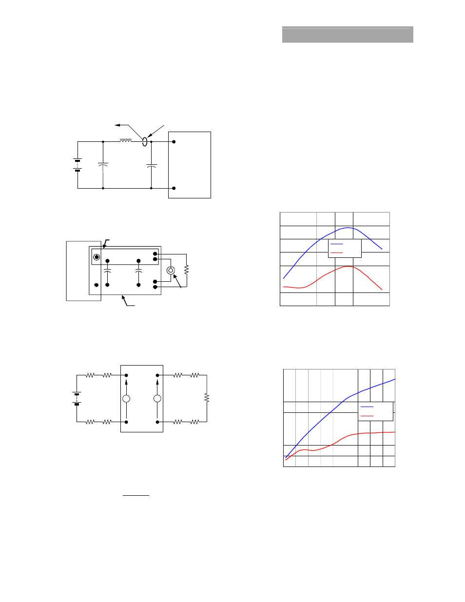
40 shows the input ripple voltage for various output
voltages at 2A of load current with 1x10 µF or 1x22 µF
ceramic capacitors and an input of 5V. Figure 41
shows the input ripple voltage for an input of 12V
In
put Ri
pple Vo
ltag
e (
m
Vp-p)
20
30
40
50
60
70
80
90
0.5
1
1.5
2
2.5
3
3.5
1x10uF
1x22uF
Output
Voltage
(Vdc)
Figure 40. Input ripple voltage for various output
voltages with 1x10 µF or 1x22 µF ceramic capacitors
at the input (2A load). Input voltage is 5V. Scope BW:
20MHz.
Input Rippl
e Vol
tag
e
(mVp-p)
20
30
40
50
60
70
80
90
100
110
0.5
1
1.5
2
2.5
3
3.5
4
4.5
5
1x10uF
1x22uF
Output
Voltage
(Vdc)
Figure 41. Input ripple voltage for various output
voltages with 1x10 µF or 1x22 µF ceramic capacitors
at the input (2A load). Input voltage is 12V. Scope BW:
20MHz