Internal schematics, Figure 4. internal schematic, Application – GE Industrial Solutions FLTR100V20 Filter Module User Manual
Page 5: Data sheet march 2008
Data Sheet
March 2008
Lineage Power
5
75 Vdc Input Maximum, 20 A Maximum
FLTR100V20 Filter Module
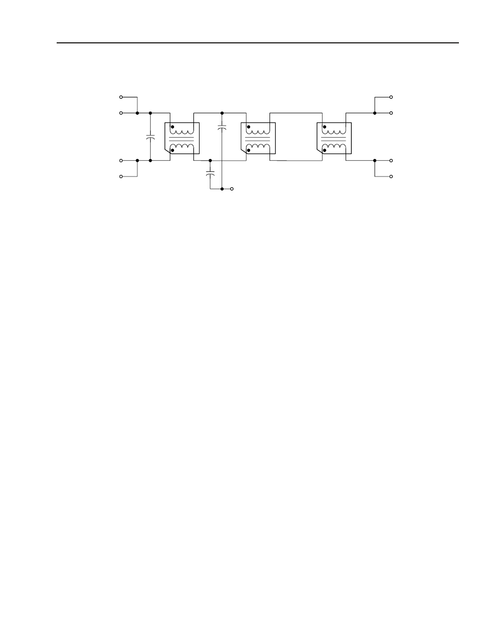
Internal Schematics
8-1324a
Figure 4. Internal Schematic
GND
V
I
(+)
V
I
(+)
V
O
V
O
V
I
(-)
V
I
(-)
V
O
V
O
(+)
(+
(-
(-
Application
Conducted noise on the input power lines can occur as
either differential-mode or common-mode noise cur-
rents. Differential-mode noise is measured between the
two input lines, and is found mostly at the low-
frequency end of the spectrum. This noise shows up as
noise at the fundamental switching frequency and its
harmonics. Common-mode noise is measured
between the input lines and ground and is mostly
broadband noise above 10 MHz. The high-frequency
nature of common-mode noise is mostly due to the
high-speed switching transitions of power train compo-
nents. Either or both types of noise may be covered in
a specification, as well as a combination of the two. An
approved measurement technique is often described,
as well.
Differential-mode noise is best attenuated using a filter
composed of line-to-line capacitors (X caps) and series
inductance, provided by either a discrete inductor or
the leakage inductance of a common-mode choke. In
addition to the differential filtering provided by the filter
module, it is recommended that an electrolytic capaci-
tor be located at the converter side of the filter to pro-
vide additional attenuation of low-frequency differential
noise and to provide a low source impedance for the
converter. This prevents input filter oscillations and
load-transient induced input voltage dips.
Common-mode noise is best attenuated by capacitors
from power module input to power module output,
capacitors from each input line to a shield plane
(Y caps), and common-mode chokes. It is recom-
mended that ceramic capacitors be added around each
power module from each input and output pin to a
shield plane under the module. The shield plane should
be connected to the CASE pin.
The GND pin of the filter module is attached to Y caps
within the module. This pin should be tied to a quiet
chassis ground point away from the power modules.
GND of the filter module should not be tied to the
CASE pin of the power module since this is a noisy
node and will inject noise into the filter, increasing the
input common-mode noise.
If no quiet grounding point is available, it is best to
leave the filter module GND pin unattached. Each
power system design will be different, and some exper-
imentation may be necessary to arrive at the best con-
figuration.
Figure 5 shows a typical schematic of a power module
with a filter module and recommended external compo-
nents. Figure 6 is a proposed layout. More than one
power module may be attached to a single filter module
as long as input current does not exceed 20 A. Figure 7
shows the recommended schematic for two power
modules attached to a single filter.
In applications where the addition of input-to-output
capacitors is undesirable, do not use C3 and C4 shown
in Figures 5 and 6, and do not use C3, C4, C8, and C9
shown in Figure 7.
In –48 V applications where the shield plane and the
power module case must be tied to a signal, remove
C1 in Figures 5 and 6, remove C1 and C6 in Figure 7,
and connect the shield plane and CASE pin to the V
I
(+)
plane.
In +48 V applications where the shield plane and the
power module case must be tied to a signal, remove
C2 in Figures 5 and 6, remove C2 and C7 in Figure 7,
and connect the shield plane and CASE pin to the V
I
(–)
plane.