Test configurations, Design considerations, Gigatlynx – GE Industrial Solutions GigaTLynx User Manual
Page 8: Input filtering, Output filtering, Lineage power 8, Figure 20. output ripple and noise test setup, The giga tlynx
Data Sheet
September 7, 2011
GigaTLynx
TM
SMT Non-isolated Power Modules:
4.5 – 14Vdc input; 0.7Vdc to 2.0Vdc, 50A Output
LINEAGE
POWER
8
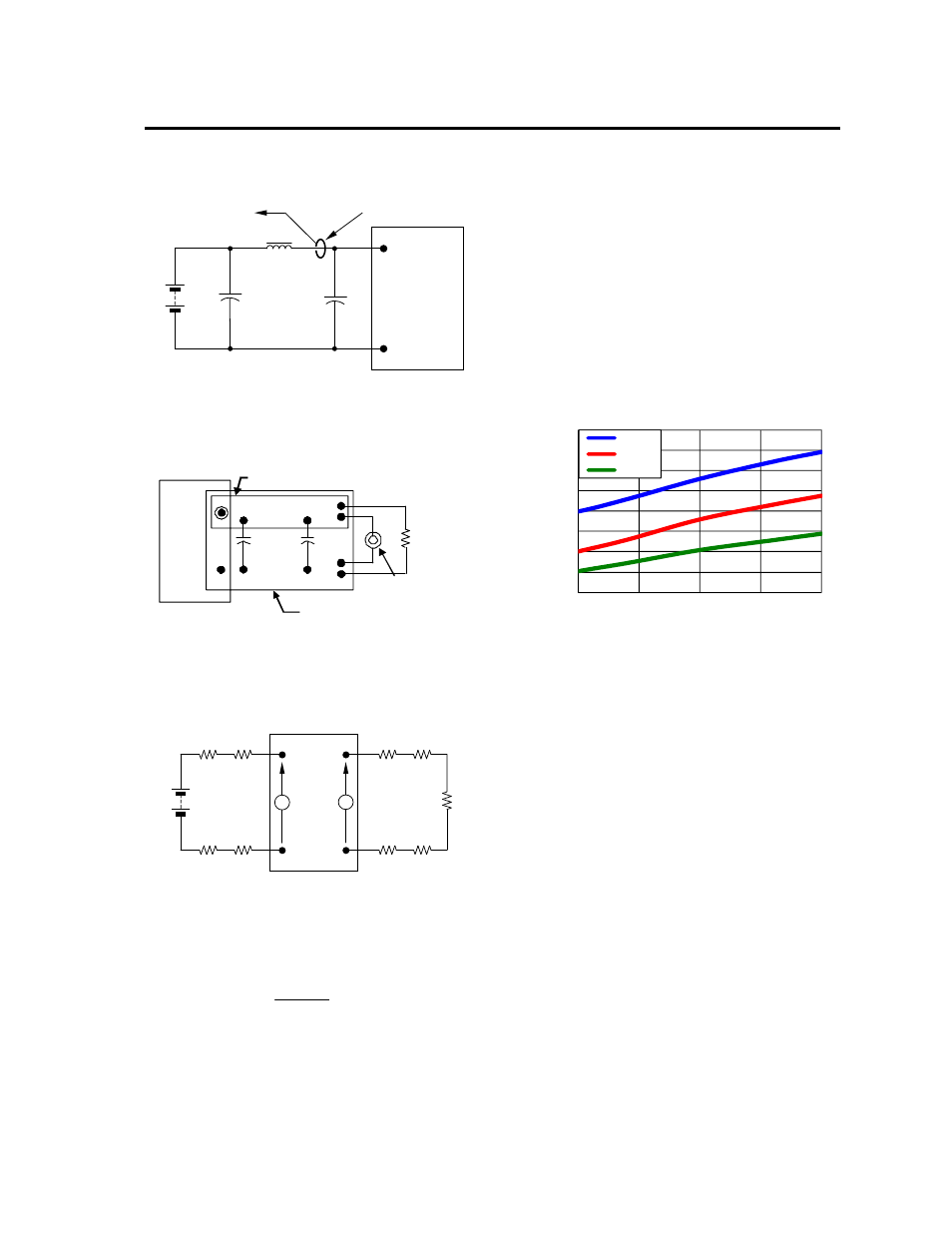
Test Configurations
TO OSCILLOSCOPE
CURRENT PROBE
L
TEST
1μH
BA
T
T
E
R
Y
C
S
1000μF
Electrolytic
E.S.R.<0.1
Ω
@ 20°C 100kHz
2x100μF
Tantalum
V
IN
(+)
COM
NOTE: Measure input reflected ripple current with a simulated
source inductance (L
TEST
) of 1μH. Capacitor C
S
offsets
possible battery impedance. Measure current as shown
above.
C
IN
Figure 19. Input Reflected Ripple Current Test Setup.
NOTE: All voltage measurements to be taken at the module
terminals, as shown above. If sockets are used then
Kelvin connections are required at the module terminals
to avoid measurement errors due to socket contact
resistance.
Vo+
COM
0.1uF
RESISTIVE
LOAD
SCOPE USING
BNC SOCKET
COPPER STRIP
GROUND PLANE
10uF
Figure 20. Output Ripple and Noise Test Setup.
V
O
COM
V
IN
(+)
COM
R
LOAD
R
contact
R
distribution
R
contact
R
distribution
R
contact
R
contact
R
distribution
R
distribution
V
IN
V
O
NOTE: All voltage measurements to be taken at the module
terminals, as shown above. If sockets are used then
Kelvin connections are required at the module terminals
to avoid measurement errors due to socket contact
resistance.
Figure 21. Output Voltage and Efficiency Test Setup.
η =
V
O
. I
O
V
IN
. I
IN
x
100
%
Efficiency
Design Considerations
Input Filtering
The Giga TLynx
TM
module should be connected to a
low ac-impedance source. A highly inductive source
can affect the stability of the module. An input
capacitance must be placed directly adjacent to the
input pin of the module, to minimize input ripple voltage
and ensure module stability.
To minimize input voltage ripple, ceramic capacitors
are recommended at the input of the module. Figure 22
shows the input ripple voltage for various output
voltages at maximum load current with 2x22 µF or
4x22 µF or 4x47 µF ceramic capacitors and an input of
12V.
Input
R
ippl
e Vol
tage
(mVp-
p
)
Output Voltage (Vdc)
Figure 22. Input ripple voltage for various output
voltages with 2x22 µF, 4x22 µF or 4x47 µF ceramic
capacitors at the input (maximum load). Input voltage
is 12V
Output Filtering
The Giga TLynx
TM
modules are designed for low output
ripple voltage and will meet the maximum output ripple
specification with 0.1 µF ceramic and 10 µF ceramic
capacitors at the output of the module. However,
additional output filtering may be required by the system
designer for a number of reasons. First, there may be a
need to further reduce the output ripple and noise of the
module. Second, the dynamic response characteristics
may need to be customized to a particular load step
change.
To reduce the output ripple and improve the dynamic
response to a step load change, additional capacitance at
the output can be used. Low ESR polymer and ceramic
capacitors are recommended to improve the dynamic
response of the module. Figure 23
provides output ripple
information for different external capacitance values at
various Vo and for full load currents. For stable
operation
of the module, limit the capacitance to less than the
maximum output capacitance as specified in the electrical
specification table. Optimal performance of the module
can be
achieved by using the Tunable Loop feature described
later in this data sheet.
50
75
100
125
150
175
200
225
250
1
1.25
1.5
1.75
2
2x22uF
4x22uF
4x47uF