Test configurations, Design considerations, Austin minilynx – GE Industrial Solutions Austin Minilynx 12V SIP User Manual
Page 10: Input filtering, Lineage power 10, Figure 24. output ripple and noise test setup
Data Sheet
October 2, 2009
Austin MiniLynx
TM
12V SIP Non-isolated Power Modules:
8.3 – 14Vdc Input; 0.75Vdc to 5.5Vdc Output; 3A output current
LINEAGE
POWER
10
Test Configurations
TO OSCILLOSCOPE
CURRENT PROBE
L
TEST
1μH
B
A
TTE
R
Y
C
S
1000μF
Electrolytic
E.S.R.<0.1
Ω
@ 20°C 100kHz
2x100μF
Tantalum
V
IN
(+)
COM
NOTE: Measure input reflected ripple current with a simulated
source inductance (L
TEST
) of 1μH. Capacitor C
S
offsets
possible battery impedance. Measure current as shown
above.
C
IN
Figure 23. Input Reflected Ripple Current Test
Setup.
NOTE: All voltage measurements to be taken at the module
terminals, as shown above. If sockets are used then
Kelvin connections are required at the module terminals
to avoid measurement errors due to socket contact
resistance.
V
O
(+)
COM
1uF
.
RESISTIVE
LOAD
SCOPE
COPPER STRIP
GROUND PLANE
10uF
Figure 24. Output Ripple and Noise Test Setup.
V
O
COM
V
IN
(+)
COM
R
LOAD
R
contact
R
distribution
R
contact
R
distribution
R
contact
R
contact
R
distribution
R
distribution
V
IN
V
O
NOTE: All voltage measurements to be taken at the module
terminals, as shown above. If sockets are used then
Kelvin connections are required at the module terminals
to avoid measurement errors due to socket contact
resistance.
Figure 25. Output Voltage and Efficiency Test
Setup.
η =
V
O
. I
O
V
IN
. I
IN
x
100
%
Efficiency
Design Considerations
Input Filtering
Austin MiniLynx
TM
12V SIP module should be
connected to a low -impedance source. A highly
inductive source can affect the stability of the module.
An input capacitance must be placed directly adjacent
to the input pin of the module, to minimize input ripple
voltage and ensure module stability in the presence of
inductive traces that supply input voltage to the
module.
In a typical application, a 22 µF low-ESR ceramic
capacitors will be sufficient to provide adequate ripple
voltage at the input of the module. To further
minimize ripple voltage at the input, additional
ceramic capacitors are recommended at the input of
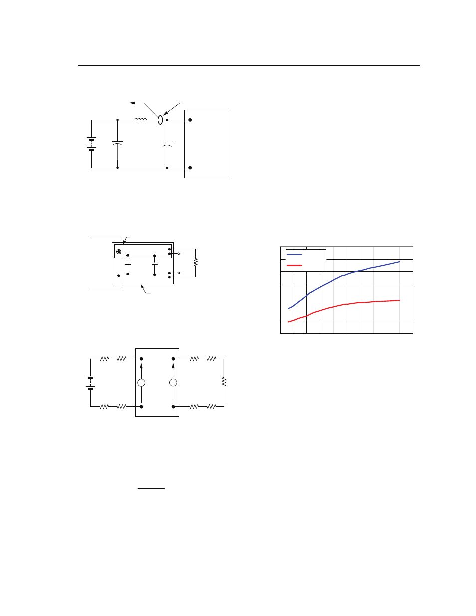
the module. Figure 26 shows input ripple voltage
(mVp-p) for various outputs with a 10 µF or a 22µF
input ceramic capacitor at full load.
0
50
100
150
200
250
300
350
0.5
1
1.5
2
2.5
3
3.5
4
4.5
5
5.5
1 x 10uF
1 x 22uF
Figure 26. Input ripple voltage for various outputs
with 10 µF or a 22 µF ceramic capacitor at the
input (full-load).