Serial controller interface, Spi interface, Spi single-cycle access – Rainbow Electronics MAX3107 User Manual
Page 44: Spi burst access, I2c interface, Start, stop, and repeated start conditions, Slave address, Spi single-cycle access spi burst access, C interface, Max3107 spi/i
44 _____________________________________________________________________________________
MAX3107
SPI/I
2
C UART with 128-Word FIFOs
and Internal Oscillator
Serial Controller Interface
The MAX3107 can be controlled through SPI or I
2
C as
defined by the logic on I2C/SPI. See the Pin Configurations
for further details.
SPI Interface
The SPI supports both single-cycle and burst-read/write
access. The SPI master must generate clock and data
signals in SPI MODE0 (i.e., with clock polarity CPOL = 0
and clock phase CPHA = 0).
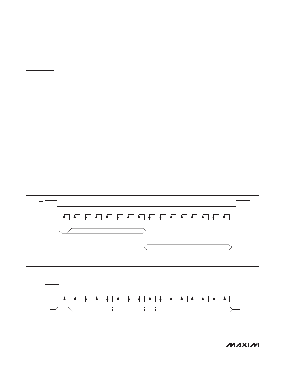
SPI Single-Cycle Access
Figure 15 shows a single-cycle read and Figure 16
shows a single-cycle write.
SPI Burst Access
In burst access, the internal SPI address is automatically
incremented. If the initial address is 0x00 [THR or RHR],
burst access does not increment the address. This
allows for block reading and writing of the FIFOs.
I
2
C Interface
The MAX3107 contains an I
2
C-compatible interface for
data communication with a host processor (SCL and
SDA). The interface supports a clock frequency up to
400kHz. SCL and SDA require pullup resistors that are
connected to a positive supply.
START, STOP, and Repeated START Conditions
When writing to the MAX3107 using I
2
C, the master
sends a START condition (S) followed by the MAX3107
I
2
C address. After the address, the master sends
the register address of the register that is to be pro-
grammed. The master then ends communication by
issuing a STOP condition (P) to relinquish control of the
bus, or a repeated START condition (Sr) to communicate
to another I
2
C slave. See Figure 17.
Slave Address
The MAX3107 includes a 7-bit slave address. The first 5
bits (MSBs) of the slave address are factory-programmed
and always 01011. These slave addresses are unique
device IDs. Connect A1, A0 to ground or V
L
to set the
I
2
C slave address (Table 5). The address is defined as
the 7 MSBs followed by the read/write bit. Set the read/
write bit to 1 to configure the MAX3107 to read mode. Set
the read/write bit to 0 to configure the MAX3107 to write
mode. The address is the first byte of information sent to
the MAX3107 after the START condition.
Figure 15. SPI Single-Cycle Read
Figure 16. SPI Single-Cycle Write
CS
R
A6
A5
A4
A3
A2
A1
A0
D7
D6
D5
D4
D3
D2
D1
D0
SCLK
SDI
SDO
A_ = REGISTER ADDRESS
D_ = 8-BIT REGISTER CONTENTS
CS
W
A6
A5
A4
A3
A2
A1
A0
D7
D6
D5
D4
D3
D2
D1
D0
SCLK
SDI
A_ = REGISTER ADDRESS
D_ = 8-BIT REGISTER CONTENTS