Rainbow Electronics MAX1717 User Manual
Page 31
MAX1717
Dynamically Adjustable, Synchronous
Step-Down Controller for Notebook CPUs
______________________________________________________________________________________
31
is at the junction of the inductor and the positioning
resistor.
7) Route high-speed switching nodes away from sensitive
analog areas (CC, REF, ILIM). Make all pin-strap
control input connections (SKP/SDN, ILIM, etc.) to ana-
log ground or V
CC
rather than power ground or V
DD
.
Layout Procedure
1) Place the power components first, with ground termi-
nals adjacent (Q2 source, CIN-, COUT-, D1 anode).
If possible, make all these connections on the top
layer with wide, copper-filled areas.
2) Mount the controller IC adjacent to MOSFET Q2,
preferably on the back side opposite Q2 in order to
keep LX-GND current-sense lines and the DL drive line
short and wide. The DL gate trace must be short and
wide, measuring 10 to 20 squares (50mils to 100mils
wide if the MOSFET is 1 inch from the controller IC).
3) Group the gate-drive components (BST diode and
capacitor, V
DD
bypass capacitor) together near the
controller IC.
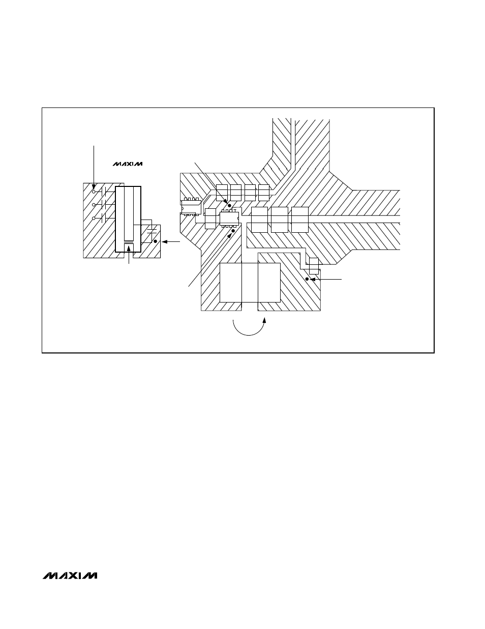
4) Make the DC-DC controller ground connections as
shown in Figure 12. This diagram can be viewed as
having three separate ground planes: output ground,
where all the high-power components go; the GND
plane, where the GND pin and V
DD
bypass capacitors
go; and an analog ground plane where sensitive
analog components go. The analog ground plane
and GND plane must meet only at a single point
directly beneath the IC. These two planes are then
connected to the high-power output ground with a
short connection from GND to the source of the low-
side MOSFET Q2 (the middle of the star ground).
This point must also be very close to the output
capacitor ground terminal.
5) Connect the output power planes (VCORE and system
ground planes) directly to the output filter capacitor
positive and negative terminals with multiple vias.
Place the entire DC-DC converter circuit as close to
the CPU as is practical.
D1
Q2
V
BATT
GND IN
COUT
VIA TO FB
AND FBS
VIA TO LX
VIA TO SOURCE
OF Q2
VIA TO GND
NEAR Q2 SOURCE
INDUCTOR DISCHARGE PATH HAS LOW DC RESISTANCE
GND
OUT
V
OUT
L1
Q1
CC
V
CC
V
DD
REF
ALL ANALOG GROUNDS
CONNECT TO LOCAL PLANE ONLY
NOTES: "STAR" GROUND IS USED.
D1 IS DIRECTLY ACROSS Q2.
CONNECT LOCAL ANALOG GROUND PLANE DIRECTLY TO GND FROM
THE SIDE OPPOSITE THE V
DD
CAPACITOR GND TO AVOID V
DD
GROUND
CURRENTS FROM FLOWING IN THE ANALOG GROUND PLANE.
MAX1717
CIN
R6
GND
Figure 12. Power-Stage PC Board Layout Example