Design procedure, Table 5. operating mode truth table – Rainbow Electronics MAX1717 User Manual
Page 24
MAX1717
Dynamically Adjustable, Synchronous
Step-Down Controller for Notebook CPUs
24
______________________________________________________________________________________
NO FAULT Test Mode
The over/undervoltage protection features can compli-
cate the process of debugging prototype breadboards
since there are (at most) a few milliseconds in which to
determine what went wrong. Therefore, a test mode is
provided to disable totally the OVP, UVP, and thermal
shutdown features, and clear the fault latch if it has
been set. The PWM operates as if SKP/SDN were high
(SKIP mode). The NO FAULT test mode is entered by
forcing 12V to 15V on SKP/SDN.
Design Procedure
Firmly establish the input voltage range and maximum
load current before choosing a switching frequency
and inductor operating point (ripple-current ratio). The
primary design trade-off lies in choosing a good switch-
ing frequency and inductor operating point, and the fol-
lowing four factors dictate the rest of the design:
1) Input Voltage Range. The maximum value (V
IN(MAX)
)
must accommodate the worst-case high AC adapter
voltage. The minimum value (V
IN(MIN)
) must account
for the lowest battery voltage after drops due to con-
nectors, fuses, and battery selector switches. If there
is a choice at all, lower input voltages result in better
efficiency.
2) Maximum Load Current. There are two values to con-
sider. The peak load current (I
LOAD(MAX)
) deter-
mines the instantaneous component stresses and
filtering requirements, and thus drives output capaci-
tor selection, inductor saturation rating, and the
design of the current-limit circuit. The continuous load
current (I
LOAD
) determines the thermal stresses and
thus drives the selection of input capacitors,
MOSFETs, and other critical heat-contributing com-
ponents. Modern notebook CPUs generally exhibit
I
LOAD
= I
LOAD(MAX)
x 80%.
3) Switching Frequency. This choice determines the
basic trade-off between size and efficiency. The opti-
mal frequency is largely a function of maximum input
voltage, due to MOSFET switching losses that are pro-
portional to frequency and V
IN2
. The optimum frequen-
cy is also a moving target, due to rapid improvements
in MOSFET technology that are making higher frequen-
cies more practical.
4) Inductor Operating Point. This choice provides trade-
offs between size vs. efficiency. Low inductor values
cause large ripple currents, resulting in the smallest
size, but poor efficiency and high output noise. The
minimum practical inductor value is one that causes
the circuit to operate at the edge of critical conduction
(where the inductor current just touches zero with
every cycle at maximum load). Inductor values lower
than this grant no further size-reduction benefit.
The MAX1717’s pulse-skipping algorithm initiates
skip mode at the critical conduction point. So, the
inductor operating point also determines the load-
current value at which PFM/PWM switchover occurs.
The optimum point is usually found between 20%
and 50% ripple current.
5) The inductor ripple current also impacts transient-
response performance, especially at low V
IN
- V
OUT
differentials. Low inductor values allow the inductor
current to slew faster, replenishing charge removed
from the output filter capacitors by a sudden load
step.
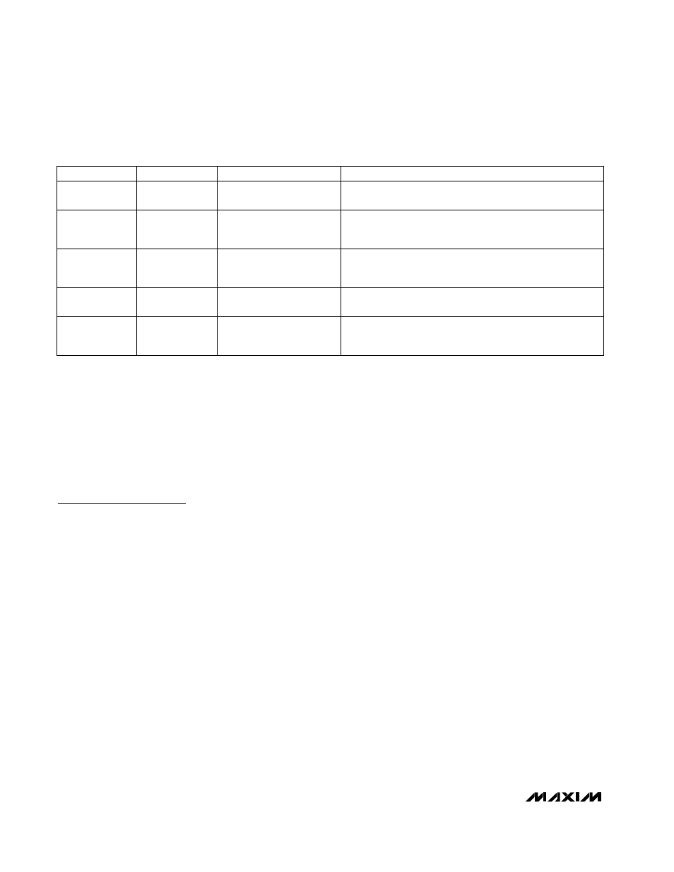
SKP/SDN
DL
MODE
COMMENT
GND
High
Shutdown
Low-power shutdown state. DL is forced to V
DD
, enforcing
OVP. I
CC
+ I
DD
= 2µA (typ).
12V to 15V
Switching
No Fault
Test mode with faults disabled and fault latches cleared, includ-
ing thermal shutdown. Otherwise, normal operation, with auto-
matic PWM/PFM switchover for pulse-skipping at light loads.
Float
Switching
Run (PWM, low noise)
Low-noise operation with no automatic switchover. Fixed-
frequency PWM action is forced regardless of load. Inductor
current reverses at light load levels.
V
CC
Switching
Run (PFM/PWM,
normal operation)
Normal operation with automatic PWM/PFM switchover for
pulse-skipping at light loads.
V
CC
or Float
High
Fault
Fault latch has been set by OVP, UVP, or thermal shutdown.
Device will remain in FAULT mode until V
CC
power is cycled or
SKP/SDN is forced low.
Table 5. Operating Mode Truth Table