Rainbow Electronics MAX1717 User Manual
Page 23
MAX1717
Dynamically Adjustable, Synchronous
Step-Down Controller for Notebook CPUs
______________________________________________________________________________________
23
The transition time is given by:
where f
SLEW
= 150kHz x 120k
Ω / R
TIME
, V
OLD
is the
original output voltage, and V
NEW
is the new output volt-
age. See Time Frequency Accuracy in the Electrical
Characteristics for f
SLEW
accuracy.
The practical range of R
TIME
is 47k
Ω to 470kΩ, corre-
sponding to 2.6µs to 26µs per 25mV step. Although the
DAC takes discrete 25mV steps, the output filter makes
the transitions relatively smooth. The average inductor
current required to make an output voltage transition is:
I
L
≅ C
OUT
x 25mV x f
SLEW
Output Overvoltage Protection
The overvoltage protection (OVP) circuit is designed to
protect against a shorted high-side MOSFET by draw-
ing high current and blowing the battery fuse. The out-
put voltage is continuously monitored for overvoltage. If
the output is more than 2.25V, OVP is triggered and the
circuit shuts down. The DL low-side gate-driver output
is then latched high until SKP/SDN is toggled or V
CC
power is cycled below 1V. This action turns on the syn-
chronous-rectifier MOSFET with 100% duty and, in turn,
rapidly discharges the output filter capacitor and forces
the output to ground. If the condition that caused the
overvoltage (such as a shorted high-side MOSFET)
persists, the battery fuse will blow. DL is also kept high
continuously when V
CC
UVLO is active, as well as in
shutdown mode (Table 5).
Overvoltage protection can be defeated through the
NO FAULT test mode (see the NO FAULT Test Mode
section).
Output Undervoltage Shutdown
The output UVP function is similar to foldback current
limiting, but employs a timer rather than a variable cur-
rent limit. If the MAX1717 output voltage is under 70% of
the nominal value, the PWM is latched off and won’t
restart until V
CC
power is cycled or SKP/SDN is tog-
gled. To allow startup, UVP is ignored during the under-
voltage fault-blanking time (the first 256 cycles of the
slew rate after startup).
UVP can be defeated through the NO FAULT test mode
(see the NO FAULT Test Mode section).
≤ µ +
+
−
4
1
1
25
s
f
V
V
mV
SLEW
OLD
NEW
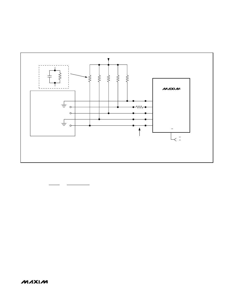
MAX1717
D4
D3
D2
D1
D0
A/B
*TO REDUCE QUIESCENT CURRENT, 1k
Ω PULLUP RESISTORS CAN BE REPLACED BY 1MΩ RESISTORS WITH 4.7nF CAPACATORS IN PARALLEL.
B-MODE VID =
01000
→ 1.6V
CPU VID =
01101
→ 1.35V
(A-MODE)
1k
Ω
1M
Ω
1k
Ω
1k
Ω
1k
Ω
1k
Ω
4.7nF
*OPTIONAL
3.15 TO 5.5V
100k
Ω
CPU
A/B = LOW = 1.60V
A/B = HIGH = 1.35V
Figure 10. Using the Internal Mux with CPU Driving the A-Mode VID Code