Block diagram, At93c86, Absolute maximum ratings – Rainbow Electronics AT93C86 User Manual
Page 2

2
AT93C86
1237D–SEEPR–08/02
Upon receiving a READ instruction at DI, the address is decoded and the data is clocked out serially on the data output pin
DO. The WRITE cycle is completely self-timed and no separate ERASE cycle is required before WRITE. The WRITE cycle
is only enabled when the part is in the ERASE/WRITE ENABLE state. When CS is brought “high” following the initiation of
a WRITE cycle, the DO pin outputs the READY/BUSY status of the part. The AT93C86 is available in a 2.7V to 5.5V
version.
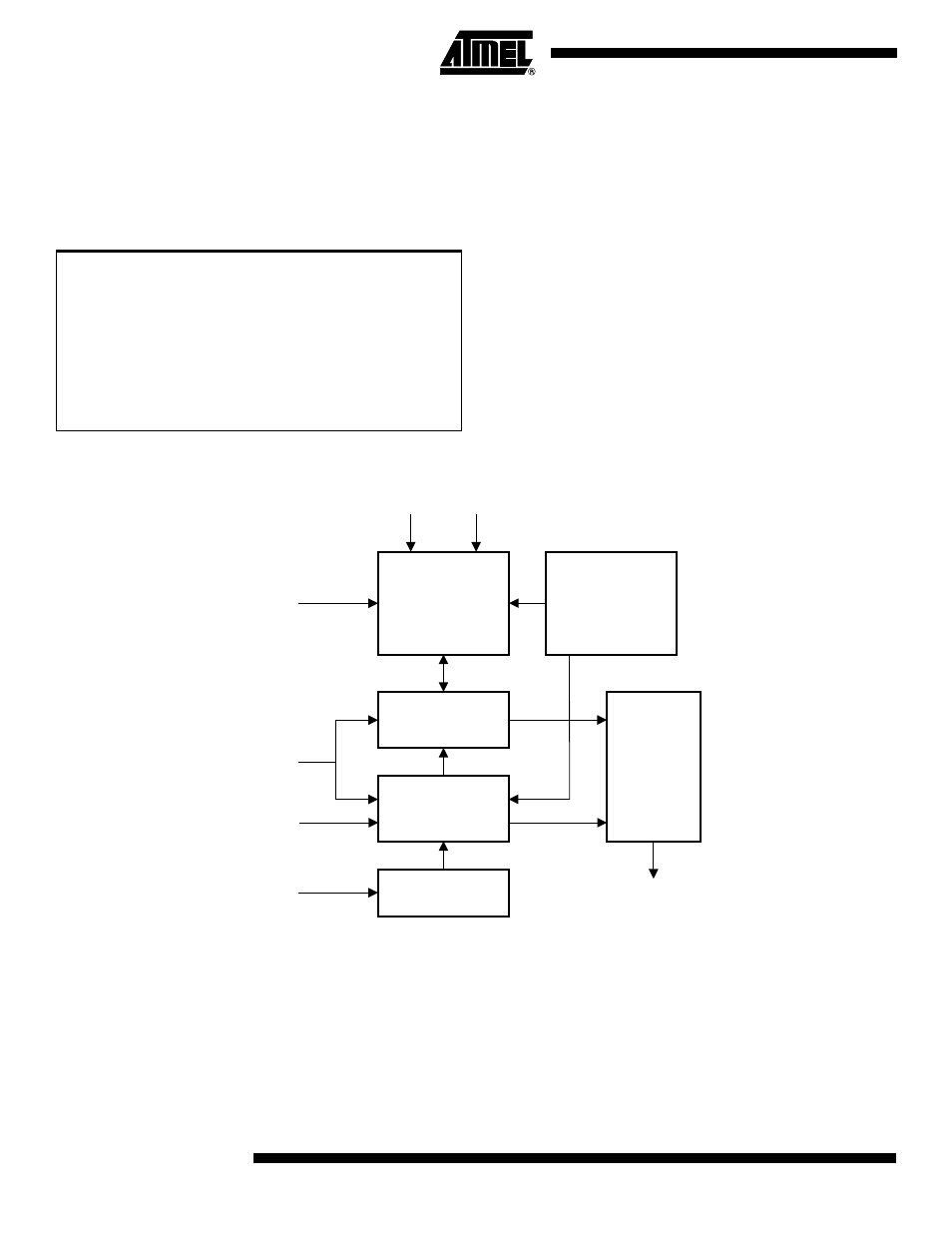
Block Diagram
Note:
1. When the ORG pin is connected to Vcc, the x 16 organization is selected. When it is connected to ground, the x 8 organiza-
tion is selected. If the ORG pin is left unconnected and the application does not load the input beyond the capability of the
internal 1 Meg ohm pullup, then the x 16 organization is selected. This feature is not available on the 1.8V devices.
Absolute Maximum Ratings*
Operating Temperature .................................. -55
°C to +125°C
*NOTICE:
Stresses beyond those listed under “Absolute
Maximum Ratings” may cause permanent dam-
age to the device. This is a stress rating only and
functional operation of the device at these or any
other conditions beyond those indicated in the
operational sections of this specification is not
implied. Exposure to absolute maximum rating
conditions for extended periods may affect
device reliability
Storage Temperature ..................................... -65
°C to +150°C
Voltage on any Pin
with Respect to Ground .....................................-1.0V to +7.0V
Maximum Operating Voltage .......................................... 6.25V
DC Output Current........................................................ 5.0 mA
ADDRESS
DECODER
OUTPUT
BUFFER
DO
ORG
DI
CS
SK
Vcc
GND
CLOCK
GENERATOR
MODE
DECODE
LOGIC
DATA
REGISTER
MEMORY ARRAY
2048 x 8
OR
1024 x 16
