Ac read waveforms, Ac read characteristics, Input test waveforms and measurement level – Rainbow Electronics Preliminary User Manual
Page 8: Output test load, Pin capacitance
AT49F004/4096A(T)
8
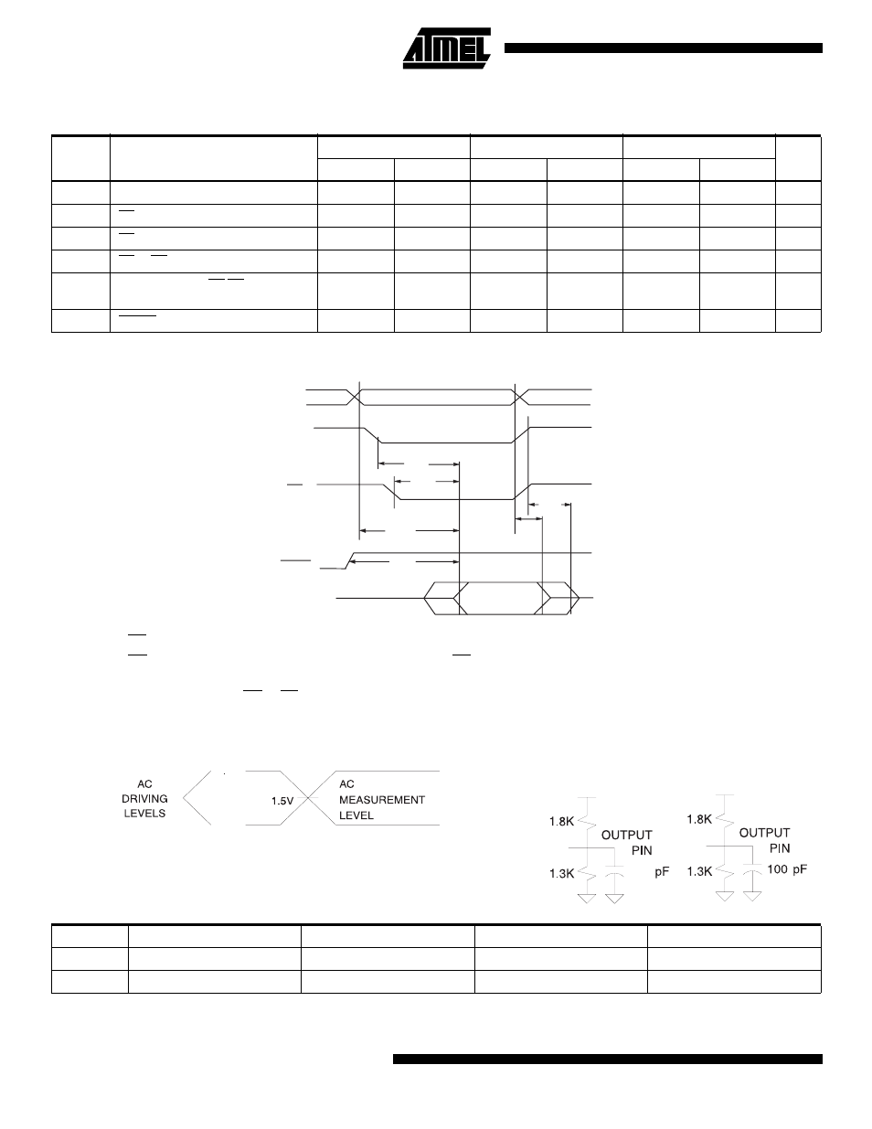
AC Read Waveforms
(1)(2)(3)(4)
Notes:
1.
CE may be delayed up to t
ACC
- t
CE
after the address transition without impact on t
ACC
.
2.
OE may be delayed up to t
CE
- t
OE
after the falling edge of CE without impact on t
CE
or by t
ACC
- t
OE
after an address change
without impact on t
ACC
.
3.
t
DF
is specified from OE or CE whichever occurs first (C
L
= 5 pF).
4.
This parameter is characterized and is not 100% tested.
AC Read Characteristics
Symbol
Parameter
AT49F004(T)/4096A(T)-55
AT49F004(T)/4096A(T)-70
AT49F004(T)/4096A(T)-90
Units
Min
Max
Min
Max
Min
Max
t
ACC
Address to Output Delay
55
70
90
ns
t
CE
(1)
CE to Output Delay
55
70
90
ns
t
OE
(2)
OE to Output Delay
0
30
0
35
0
40
ns
t
DF
(3)(4)
CE or OE to Output Float
0
25
0
25
0
25
ns
t
OH
Output Hold from OE,CE or Address,
whichever occurred first
0
0
0
ns
t
RO
RESET to Output Delay
800
800
800
ns
OE
RESET
CE
t
CE
t
OE
t
RO
t
ACC
t
DF
t
OH
ADDRESS
HIGH Z
OUTPUT
OUTPUT
ADDRESS VALID
VALID
Input Test Waveforms and Measurement Level
t
R
, t
F
< 5 ns
3.0V
0.0V
Output Test Load
5.0V
5.0V
90 ns
55/70 ns
30
Note:
1. This parameter is characterized and is not 100% tested.
Pin Capacitance
f = 1 MHz, T = 25
°
C
(1)
Symbol
Typ
Max
Units
Conditions
C
IN
4
6
pF
V
IN
= 0V
C
OUT
8
12
pF
V
OUT
= 0V