Rainbow Electronics Preliminary User Manual
Page 2
AT49F004/4096A(T)
2
block of data and then programming on a byte-by-byte or
word-by-word basis.
The device is erased by executing the erase command
sequence; the device internally controls the erase opera-
tion. The memory is divided into four blocks for erase oper-
ations. There are two 4K word parameter block sections,
the boot block, and the main memory array block. The typi-
cal number of program and erase cycles is in excess of
10,000 cycles.
The 8K word boot block section includes a reprogramming
lock out feature to provide data integrity. This feature is
enabled by a command sequence. Once the boot block
programming lockout feature is enabled, the data in the
boot block cannot be changed when input levels of 5.5
volts or less are used. The boot sector is designed to con-
tain user secure code.
For the AT49F4096A(T), the BYTE pin controls whether
the device data I/O pins operate in the byte or word config-
uration. If the BYTE pin is set at a logic “1” or left open, the
device is in word configuration, I/O0 - I/O15 are active and
controlled by CE and OE.
If the BYTE pin is set at logic “0”, the device is in byte con-
figuration, and only data I/O pins I/O0 - I/O7 are active and
controlled by CE and OE. The data I/O pins I/O8 - I/O14
are tri-stated and the I/O15 pin is used as an input for the
LSB (A-1) address function.
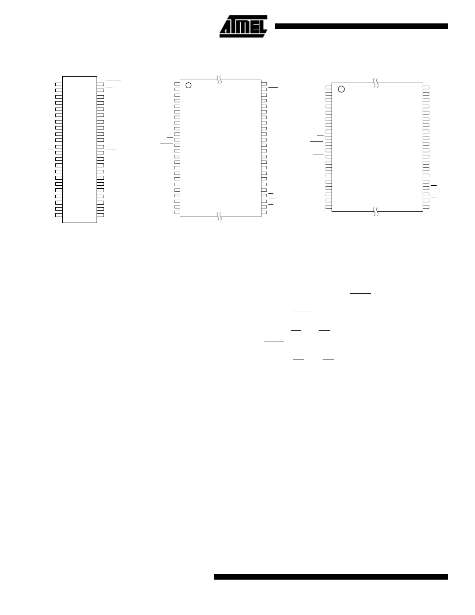
AT49F4096A(T) TSOP Top View
Type 1
1
2
3
4
5
6
7
8
9
10
11
12
13
14
15
16
17
18
19
20
21
22
23
24
48
47
46
45
44
43
42
41
40
39
38
37
36
35
34
33
32
31
30
29
28
27
26
25
A15
A14
A13
A12
A11
A10
A9
A8
NC
NC
WE
RESET
NC
NC
NC
NC
A17
A7
A6
A5
A4
A3
A2
A1
A16
BYTE
GND
I/O15 / A-1
I/O7
I/O14
I/O6
I/O13
I/O5
I/O12
I/O4
VCC
I/O11
I/O3
I/O10
I/O2
I/O9
I/O1
I/O8
I/O0
OE
GND
CE
A0
AT49F004(T) TSOP Top View
Type 1
1
2
3
4
5
6
7
8
9
10
11
12
13
14
15
16
17
18
19
20
40
39
38
37
36
35
34
33
32
31
30
29
28
27
26
25
24
23
22
21
A16
A15
A14
A13
A12
A11
A9
A8
WE
RESET
NC
RDY/BUSY
A18
A7
A6
A5
A4
A3
A2
A1
A17
GND
NC
NC
A10
I/O7
I/O6
I/O5
I/O4
VCC
VCC
NC
I/O3
I/O2
I/O1
I/O0
OE
GND
CE
A0
AT49F4096A(T) SOIC (SOP)
1
2
3
4
5
6
7
8
9
10
11
12
13
14
15
16
17
18
19
20
21
22
44
43
42
41
40
39
38
37
36
35
34
33
32
31
30
29
28
27
26
25
24
23
NC
NC
A17
A7
A6
A5
A4
A3
A2
A1
A0
CE
GND
OE
I/O0
I/O8
I/O1
I/O9
I/O2
I/O10
I/O3
I/O11
RESET
WE
A8
A9
A10
A11
A12
A13
A14
A15
A16
BYTE
GND
I/O15/A-1
I/O7
I/O14
I/O6
I/O13
I/O5
I/O12
I/O4
VCC