Memory organization, Pin capacitance – Rainbow Electronics AT24C16A User Manual
Page 3
3
AT24C02A/04A/08A/16A
0976D–12/01
The AT24C08A only uses the A2 input for hardwire addressing and a total of two 8K
devices may be addressed on a single bus system. The A0 and A1 pins are no-
connects.
The AT24C16A does not use the device address pins, which limits the number of
devices on a single bus to one. The A0, A1 and A2 pins are no-connects.
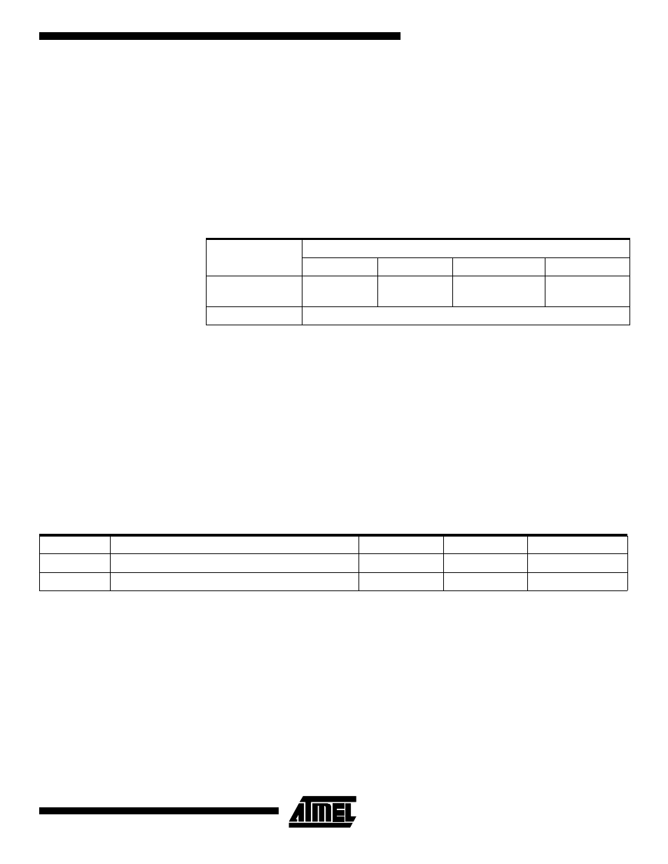
WRITE PROTECT (WP): The AT24C02A/04A/08A/16A have a Write Protect pin that
provides hardware data protection. The Write Protect pin allows normal read/write oper-
ations when connected to ground (GND). When the Write Protect pin is connected to
V
CC
, the write protection feature is enabled and operates as shown in the following
table.
Memory Organization
AT24C02A, 2K SERIAL EEPROM: Internally organized with 32 pages of 8 bytes each,
the 2K requires an 8-bit data word address for random word addressing.
AT24C04A, 4K SERIAL EEPROM: The 4K is internally organized with 32 pages of 16
bytes each. Random word addressing requires a 9-bit data word address.
AT24C08A, 8K SERIAL EEPROM: The 8K is internally organized with 64 pages of 16
bytes each. Random word addressing requires a 10-bit data word address.
AT24C16A, 16K SERIAL EEPROM: The 16K is internally organized with 128 pages of
16 bytes each. Random word addressing requires an 11-bit data word address.
Note:
1. This parameter is characterized and is not 100% tested.
WP Pin
Status
Part of the Array Protected
24C02A
24C04A
24C08A
24C16A
At V
CC
Upper Half
(1K) Array
Upper Half
(2K) Array
Full (8K)
Array
Full (16K)
Array
At GND
Normal Read/Write Operations
Pin Capacitance
Applicable over recommended operating range from T
A
= 25
°C, f = 1.0 MHz, V
CC
= +1.8V.
Symbol
Test Condition
Max
Units
Conditions
C
I/O
Input/Output Capacitance (SDA)
8
pF
V
I/O
= 0V
C
IN
Input Capacitance (A
0
, A
1
, A
2
, SCL)
6
pF
V
IN
= 0V