Rainbow Electronics AT25640A User Manual
Page 8
8
AT25080A/160A/320A/640A
3401C–SEEPR–8/04
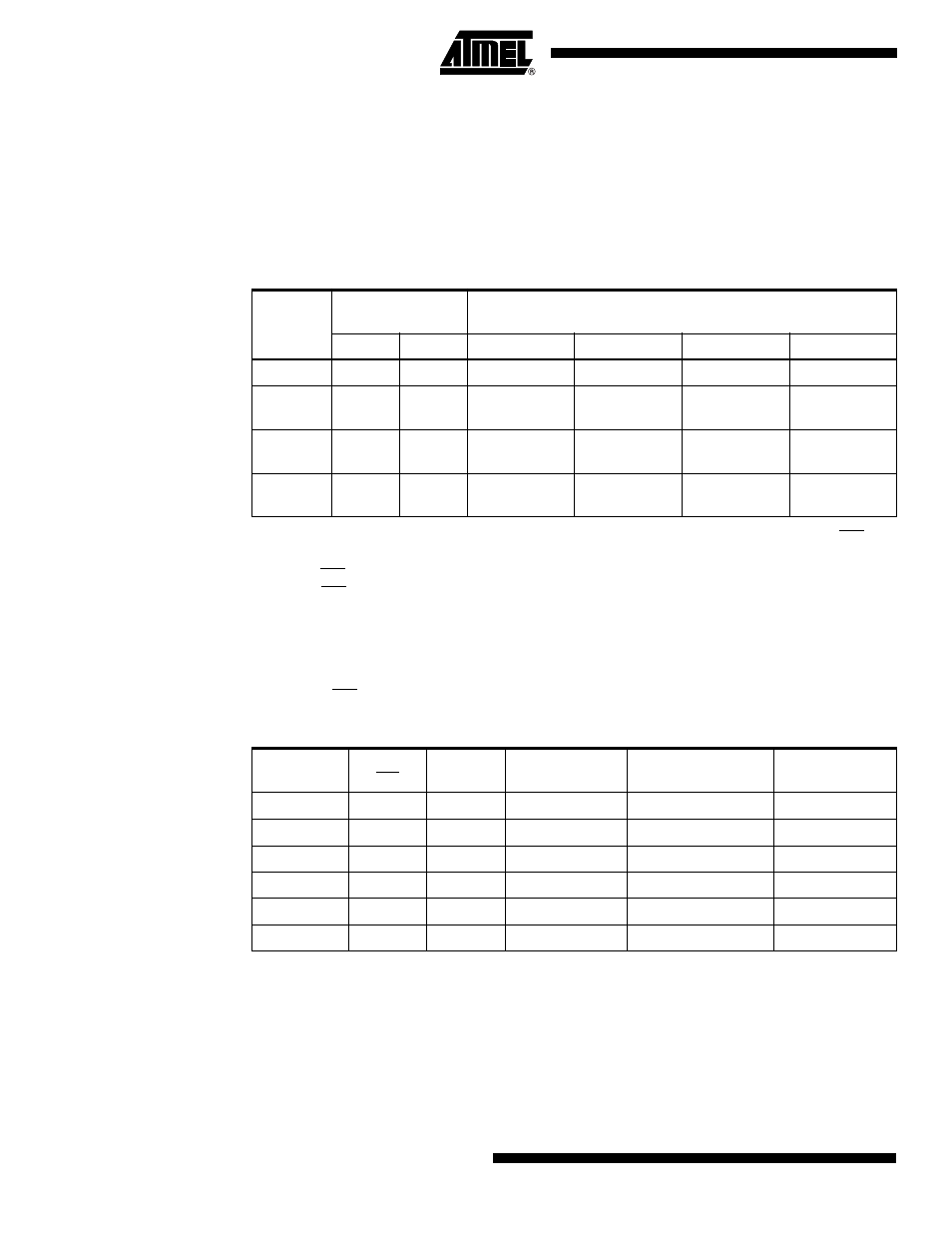
WRITE STATUS REGISTER (WRSR): The WRSR instruction allows the user to select one of
four levels of protection. The AT25080A/160A/320A/640A is divided into four array segments.
One-quarter, one-half, or all of the memory segments can be protected. Any of the data within
any selected segment will therefore be read-only. The block write protection levels and corre-
sponding status register control bits are shown in Table 8.
The three bits BP0, BP1, and WPEN are nonvolatile cells that have the same properties and
functions as the regular memory cells (e.g., WREN, t
WC
, RDSR).
The WRSR instruction also allows the user to enable or disable the write protect (WP) pin
through the use of the Write Protect Enable (WPEN) bit. Hardware write protection is enabled
when the WP pin is low and the WPEN bit is “1”. Hardware write protection is disabled when
either the WP pin is high or the WPEN bit is “0”. When the device is hardware write-protected,
writes to the status register, including the block protect bits and the WPEN bit, and the block-
protected sections in the memory array are disabled. Writes are only allowed to sections of the
memory that are not block-protected.
NOTE: When the WPEN bit is hardware write-protected, it cannot be changed back to “0” as
long as the WP pin is held low.
Table 8. Block Write Protect Bits
Level
Status
Register Bits
Array Addresses Protected
BP1
BP0
AT25080A
AT25160A
AT25320A
AT25640A
0
0
0
None
None
None
None
1(1/4)
0
1
0300
−
03FF
0600
−
07FF
0C00
−
0FFF
1800
−
1FFF
2(1/2)
1
0
0200
−
03FF
0400
−
07FF
0800
−
0FFF
1000
−
1FFF
3(All)
1
1
0000
−
03FF
0000
−
07FF
0000
−
0FFF
0000
−
1FFF
Table 9. WPEN Operation
WPEN
WP
WEN
Protected
Blocks
Unprotected
Blocks
Status
Register
0
X
0
Protected
Protected
Protected
0
X
1
Protected
Writable
Writable
1
Low
0
Protected
Protected
Protected
1
Low
1
Protected
Writable
Protected
X
High
0
Protected
Protected
Protected
X
High
1
Protected
Writable
Writable