Block diagram device operation – Rainbow Electronics AT29LV256 User Manual
Page 2
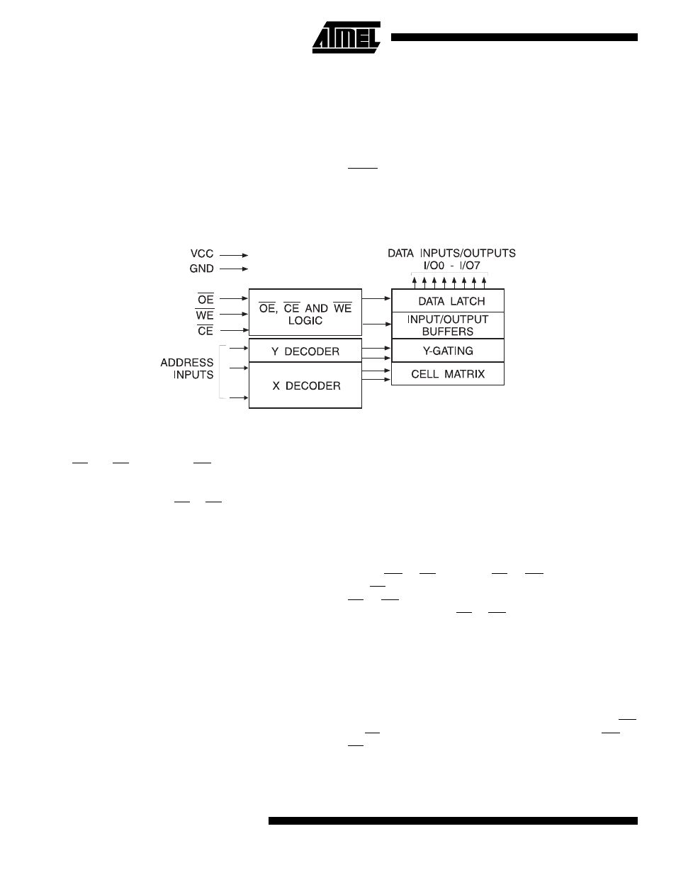
AT29LV256
2
To allow for simple in-system reprogrammability, the
AT29LV256 does not require high input voltages for pro-
gramming. Three-volt-only commands determine the oper-
ation of the device. Reading data out of the device is similar
t o r e a d i n g f r o m a n E P R O M . R e p r o g r a m m i n g t h e
AT29LV256 is performed on a sector basis; 64 bytes of
data are loaded into the device and then simultaneously
programmed.
During a reprogram cycle, the address locations and 64
bytes of data are captured at microprocessor speed and
internally latched, freeing the address and data bus for
other operations. Following the initiation of a program
cycle, the device will automatically erase the sector and
then program the latched data using an internal control
timer. The end of a program cycle can be detected by
DATA polling of I/O7. Once the end of a program cycle has
been detected, a new access for a read or program can
begin.
Block Diagram
Device Operation
READ:
The AT29LV256 is accessed like an EPROM.
When CE and OE are low and WE is high, the data stored
at the memory location determined by the address pins is
asserted on the outputs. The outputs are put in the high
impedance state whenever CE or OE is high. This dual-line
control gives designers flexibility in preventing bus conten-
tion.
SOFTWARE DATA PROTECTION PROGRAMMING: The
AT29LV256 has 512 individual sectors, each 64 bytes.
Using the software data protection feature, byte loads are
used to enter the 64 bytes of a sector to be programmed.
The AT29LV256 can only be programmed or repro-
grammed using the software data protection feature. The
device is programmed on a sector basis. If a byte of data
within the sector is to be changed, data for the entire 64-
b y t e s e c t o r m u s t b e l o a d e d i n t o t h e d e v i c e . T h e
AT29LV256 automatically does a sector erase prior to
loading the data into the sector. An erase command is not
required.
Software data protection protects the device from inadvert-
ent programming. A series of three program commands to
specific addresses with specific data must be presented to
the device before programming may occur. The same three
program commands must begin each program operation.
All software program commands must obey the sector pro-
gram timing specifications. Power transitions will not reset
the software data protection feature, however the software
feature will guard against inadvertent program cycles dur-
ing power transitions.
Any attempt to write to the device without the 3-byte com-
mand sequence will start the internal write timers. No data
will be written to the device; however, for the duration of
t
WC
, a read operation will effectively be a polling operation.
After the software data protection’s 3-byte command code
is given, a byte load is performed by applying a low pulse
on the WE or CE input with CE or WE low (respectively)
and OE high. The address is latched on the falling edge of
CE or WE, whichever occurs last. The data is latched by
the first rising edge of CE or WE.
The 64 bytes of data must be loaded into each sector. Any
byte that is not loaded during the programming of its sector
will be erased to read FFh. Once the bytes of a sector are
loaded into the device, they are simultaneously pro-
grammed during the internal programming period. After the
first data byte has been loaded into the device, successive
bytes are entered in the same manner. Each new byte to
be programmed must have its high to low transition on WE
(or CE) within 150
µ
s of the low to high transition of WE (or
CE) of the preceding byte. If a high to low transition is not
detected within 150
µ
s of the last low to high transition, the
load period will end and the internal programming period