Rainbow Electronics AT29LV256 User Manual
Features, Description, Pin configurations
1
Features
•
Single Supply Voltage, Range 3V to 3.6V
•
3-Volt Only Read and Write Operation
•
Software Protected Programming
•
Low Power Dissipation
– 15 mA Active Current
– 40 µA CMOS Standby Current
•
Fast Read Access Time - 150 ns
•
Sector Program Operation
– Single Cycle Reprogram (Erase and Program)
– 512 Sectors (64 bytes/sector)
– Internal Address and Data Latches for 64 Bytes
•
Fast Sector Program Cycle Time - 20 ms Max.
•
Internal Program Control and Timer
•
DATA Polling for End of Program Detection
•
Typical Endurance > 10,000 Cycles
•
CMOS and TTL Compatible Inputs and Outputs
•
Commercial and Industrial Temperature Ranges
Description
The AT29LV256 is a 3-volt-only in-system Flash Programmable Erasable Read Only
Memory (PEROM). Its 256K of memory is organized as 32,768 words by 8 bits. Man-
ufactured with Atmel’s advanced nonvolatile CMOS technology, the device offers
access times to 150 ns with power dissipation of just 54 mW over the commercial tem-
perature range. When the device is deselected, the CMOS standby current is less
than 40
µ
A. The device endurance is such that any sector can typically be written to in
excess of 10,000 times.
256K (32K x 8)
3-volt Only
Flash Memory
AT29LV256
Rev. 0563B–10/98
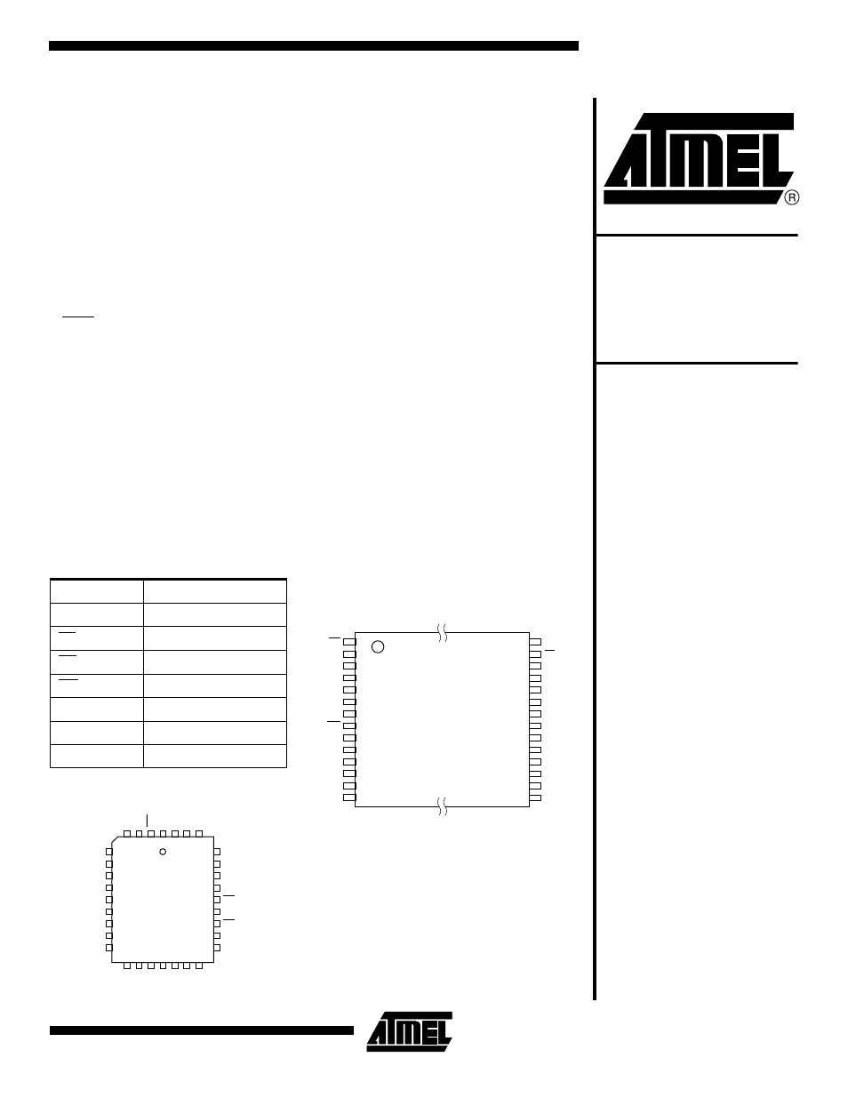
Pin Configurations
Pin Name
Function
A0 - A14
Addresses
CE
Chip Enable
OE
Output Enable
WE
Write Enable
I/O0 - I
/O7
Data Inputs/Outputs
NC
No Connect
DC
Don’t Connect
PLCC Top View
5
6
7
8
9
10
11
12
13
29
28
27
26
25
24
23
22
21
A6
A5
A4
A3
A2
A1
A0
NC
I/O0
A8
A9
A11
NC
OE
A10
CE
I/O7
I/O6
4
3
2
1
32
31
30
14
15
16
17
18
19
20
I/O1
I/O2
GND
DC
I/O3
I/O4
I/O5
A7
A12
WE
DC
VCC
A14
A13
(continued)
TSOP Top View
Type 1
22
23
24
25
26
27
28
1
2
3
4
5
6
7
21
20
19
18
17
16
15
14
13
12
11
10
9
8
OE
A11
A9
A8
A13
A14
VCC
WE
A12
A7
A6
A5
A4
A3
A10
CE
I/O7
I/O6
I/O5
I/O4
I/O3
GND
I/O2
I/O1
I/O0
A0
A1
A2