Rainbow Electronics AT25F4096 User Manual
Page 4
4
AT25F4096 [Advance Information]
2454C–SEEPR–8/04
Notes:
1. The programming time for n bytes will be equal to n x t
BPC
.
2. This parameter is characterized at 3.0V, 25
°
C and is not 100% tested.
3. One write cycle consists of erasing a sector, followed by programming the same sector.
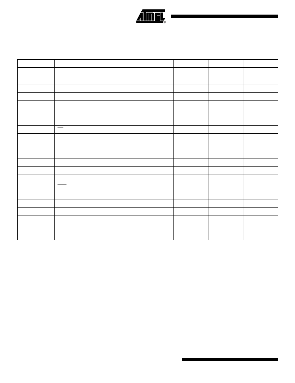
AC Characteristics (Preliminary – Subject to Change)
Applicable over recommended operating range from T
A
= -40
°
C to +85
°
C, V
CC
= +2.7V to +3.6V
C
L
= 1 TTL Gate and 30 pF (unless otherwise noted).
Symbol
Parameter
Min
Typ
Max
Units
f
SCK
SCK Clock Frequency
0
20
MHz
t
RI
Input Rise Time
20
ns
t
FI
Input Fall Time
20
ns
t
WH
SCK High Time
20
ns
t
WL
SCK Low Time
20
ns
t
CS
CS High Time
25
ns
t
CSS
CS Setup Time
25
ns
t
CSH
CS Hold Time
25
ns
t
SU
Data In Setup Time
5
ns
t
H
Data In Hold Time
5
ns
t
HD
Hold Setup Time
15
ns
t
CD
Hold Hold Time
15
ns
t
V
Output Valid
20
ns
t
HO
Output Hold Time
0
ns
t
LZ
Hold to Output Low Z
200
ns
t
HZ
Hold to Output High Z
200
ns
t
DIS
Output Disable Time
100
ns
t
EC
Erase Cycle Time per Sector
1.0
s
t
SR
Status Register Write Cycle Time
60
ms
t
BPC
Byte Program Cycle Time
(1)
30
50
µs
Endurance
(2)
10K
Write Cycles
(3)