Input diagram, Speed/power management, I/o diagram – Rainbow Electronics ATF1508ASVL User Manual
Page 7: Atf1508asv(l)
7
ATF1508ASV(L)
1408F–PLD–10/02
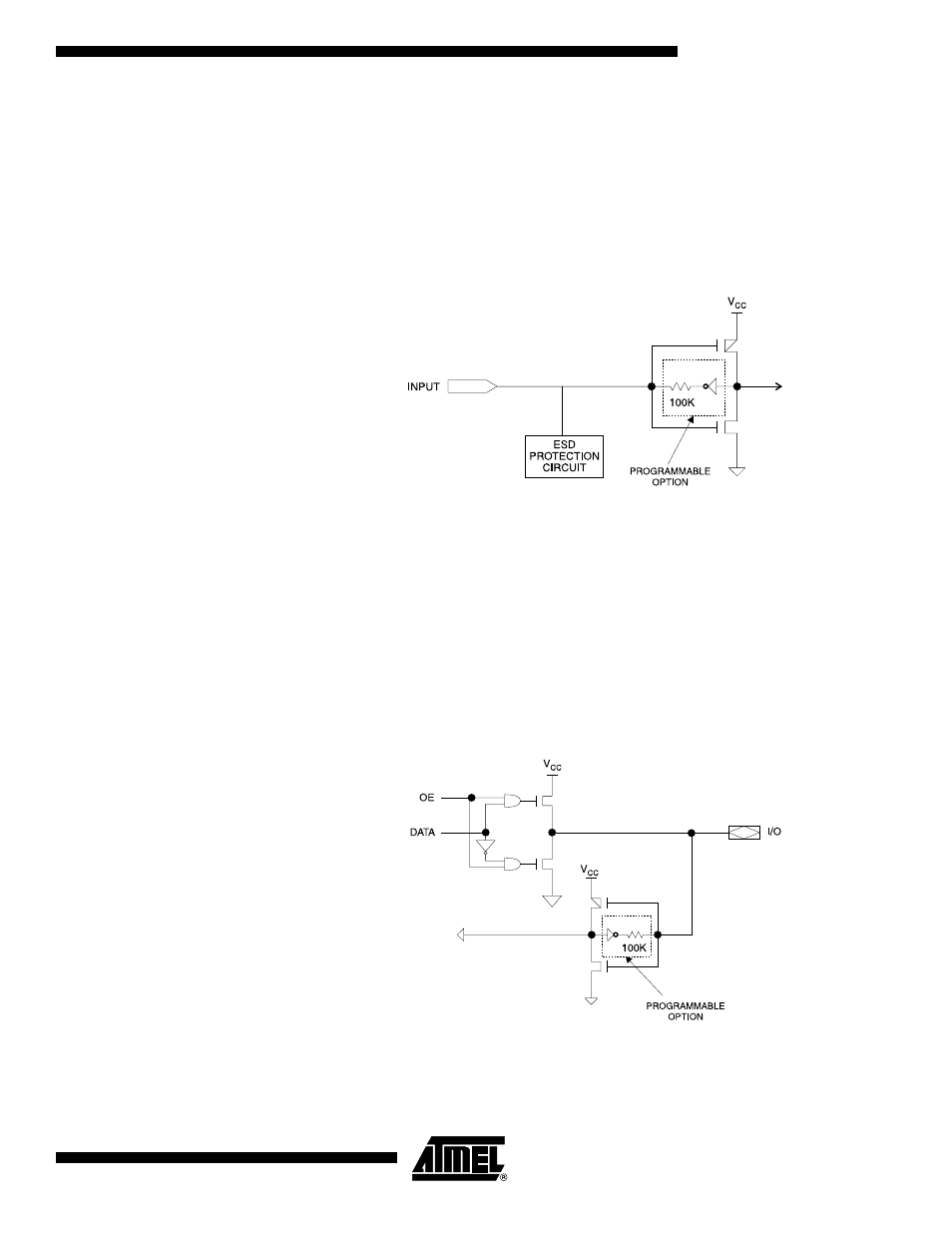
Programmable Pin-
keeper Option for
Inputs and I/Os
The ATF1508ASV(L) offers the option of programming all input and I/O pins so that “pin-
keeper” circuits can be utilized. When any pin is driven high or low and then subse-
quently left floating, it will stay at that previous high- or low-level. This circuitry prevents
unused input and I/O lines from floating to intermediate voltage levels, which causes
unnecessary power consumption and system noise. The keeper circuits eliminate the
need for external pull-up resistors and eliminate their DC power consumption.
Input Diagram
Speed/Power
Management
The ATF1508ASV(L) has several built-in speed and power management features. The
ATF1508ASV(L) contains circuitry that automatically puts the device into a low-power
standby mode when no logic transitions are occurring. This not only reduces power con-
sumption during inactive periods, but also provides proportional power-savings for most
applications running at system speeds below 5 MHz.
To further reduce power, each ATF1508ASV(L) macrocell has a reduced-power bit fea-
ture. This feature allows individual macrocells to be configured for maximum power-
savings. This feature may be selected as a design option.
I/O Diagram