Output ac test loads, Power-down mode, Power down ac characteristics(1)(2) – Rainbow Electronics ATF1508ASVL User Manual
Page 14: Atf1508asv(l), Output ac test loads power-down mode, Power down ac characteristic s
14
ATF1508ASV(L)
1408F–PLD–10/02
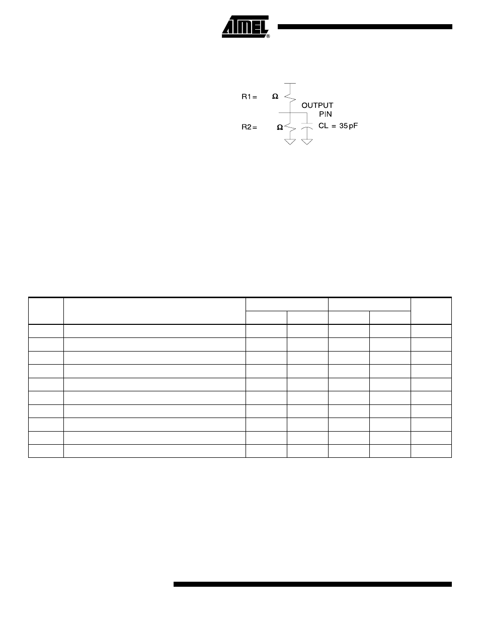
Output AC Test Loads
Power-down Mode
The ATF1508ASV(L) includes two pins for optional pin-controlled power-down feature.
When this mode is enabled, the PD pin acts as the power-down pin. When the PD1 and
PD2 pin is high, the device supply current is reduced to less than 5 mA. During power-
down, all output data and internal logic states are latched and held. Therefore, all regis-
tered and combinatorial output data remain valid. Any outputs that were in a high-Z state
at the onset will remain at high-Z. During power-down, all input signals except the
power-down pin are blocked. Input and I/O hold latches remain active to ensure that
pins do not float to indeterminate levels, further reducing system power. The power-
down pin feature is enabled in the logic design file. Designs using either power-down pin
may not use the PD pin logic array input. However, buried logic resources in this macro-
cell may still be used.
Notes:
1. For slow slew outputs, add t
SSO
.
2. Pin or product term.
3.0V
703
8060
Power Down AC Characteristics
(1)(2)
Symbol
Parameter
-15
-20
Units
Min
Max
Min
Max
t
IVDH
Valid I, I/O before PD High
15
20
ns
t
GVDH
Valid OE
(2)
before PD High
15
20
ns
t
CVDH
Valid Clock
(2)
before PD High
15
20
ns
t
DHIX
I, I/O Don’t Care after PD High
25
30
ns
t
DHGX
OE
(2)
Don’t Care after PD High
25
30
ns
t
DHCX
Clock
(2)
Don’t Care after PD High
25
30
ns
t
DLIV
PD Low to Valid I, I/O
1
1
µs
t
DLGV
PD Low to Valid OE (Pin or Term)
1
1
µs
t
DLCV
PD Low to Valid Clock (Pin or Term)
1
1
µs
t
DLOV
PD Low to Valid Output
1
1
µs