Absolute maximum ratings, Timing model, Atf1508asv(l) – Rainbow Electronics ATF1508ASVL User Manual
Page 11: Timing model absolute maximum ratings
11
ATF1508ASV(L)
1408F–PLD–10/02
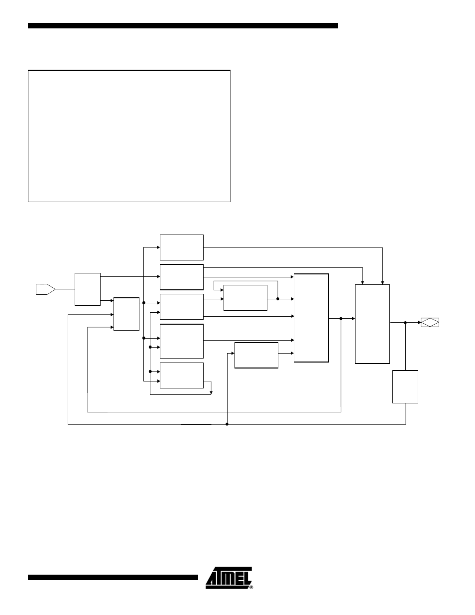
Timing Model
Absolute Maximum Ratings*
Temperature Under Bias .................................. -40°C to +85°C
*NOTICE:
Stresses beyond those listed under “Absolute
Maximum Ratings” may cause permanent dam-
age to the device. This is a stress rating only and
functional operation of the device at these or any
other conditions beyond those indicated in the
operational sections of this specification is not
implied. Exposure to absolute maximum rating
conditions for extended periods may affect device
reliability.
Note:
1.
Minimum voltage is -0.6V DC, which may under-
shoot to -2.0V for pulses of less than 20 ns. Max-
imum output pin voltage is V
CC
+ 0.75V DC,
which may overshoot to 7.0V for pulses of less
than 20 ns.
Storage Temperature ..................................... -65°C to +150°C
Voltage on Any Pin with
Respect to Ground .........................................-2.0V to +7.0V
(1)
Voltage on Input Pins
with Respect to Ground
During Programming.....................................-2.0V to +14.0V
(1)
Programming Voltage with
Respect to Ground .......................................-2.0V to +14.0V
(1)
Input
Delay
t
IN
Switch
Matrix
t
UIM
Internal Output
Enable Delay
t
IOE
Global Control
Delay
t
GLOB
Logic Array
Delay
t
LAD
Register Control
Delay
t
LAC
t
IC
t
EN
Cascade Logic
Delay
t
PEXP
Fast Input
Delay
t
FIN
Register
Delay
t
SU
t
H
t
PRE
t
CLR
t
RD
t
COMB
t
FSU
t
FH
Output
Delay
t
OD1
t
OD2
t
OD3
t
XZ
t
ZX1
t
ZX2
t
ZX3
I/O Delay
t
IO
Foldback Term
Delay
t
SEXP