Dc and ac operating conditions, Dc characteristics, Pin capacitance – Rainbow Electronics ATF1508ASVL User Manual
Page 10: Atf1508asv(l)
10
ATF1508ASV(L)
1408F–PLD–10/02
Notes:
1. Not more than one output at a time should be shorted. Duration of short circuit test should not exceed 30 sec.
2. I
CC3
refers to the current in the reduced-power mode when macrocell reduced-power is turned ON.
Note:
Typical values for nominal supply voltage. This parameter is only sampled and is not 100% tested. The OGI pin (high-voltage pin
during programming) has a maximum capacitance of 12 pF.
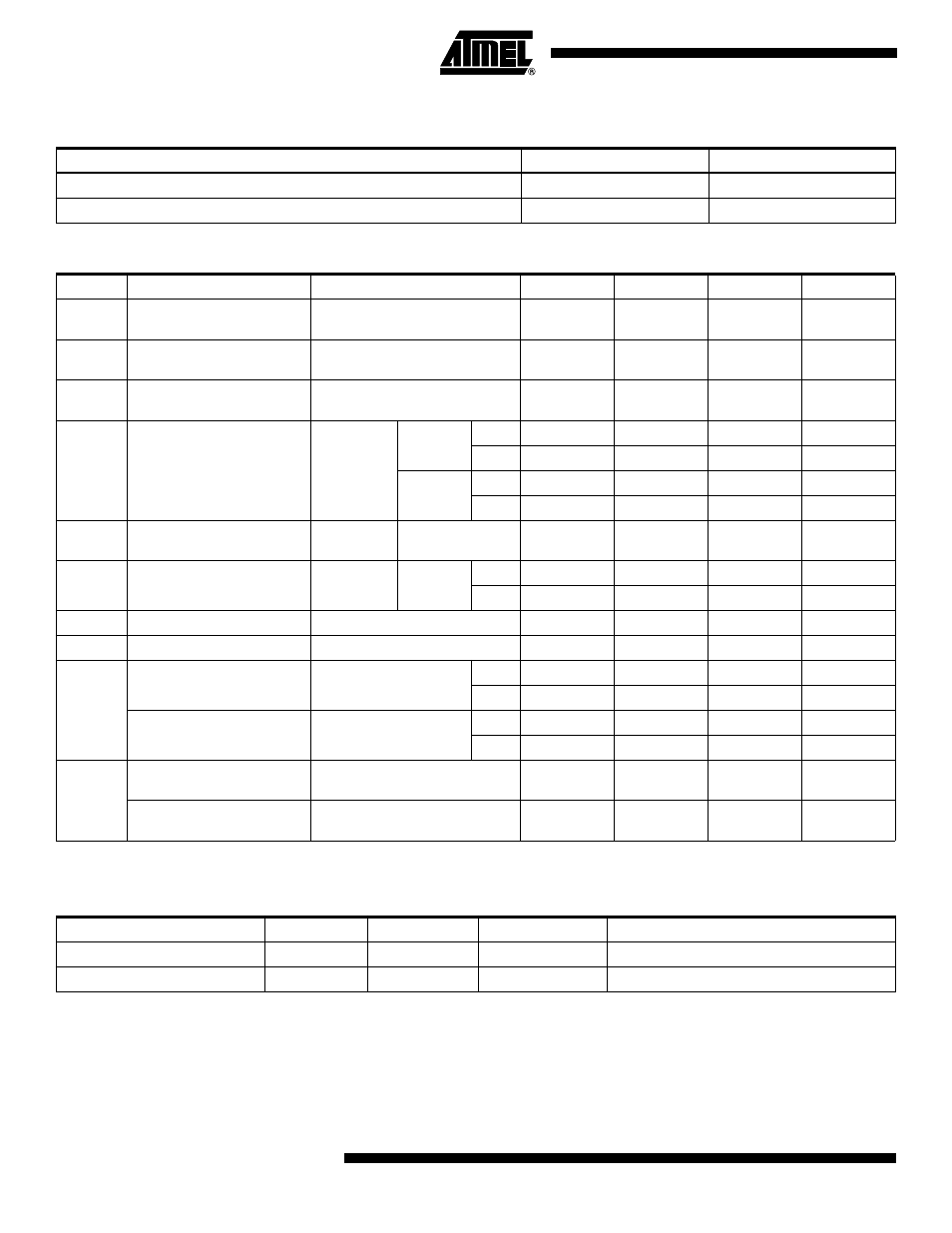
DC and AC Operating Conditions
Commercial
Industrial
Operating Temperature (Ambient)
0°C - 70°C
-40°C - 85°C
V
CC
(3.3V) Power Supply
3.0V - 3.6V
3.0V - 3.6V
DC Characteristics
Symbol
Parameter
Condition
Min
Typ
Max
Units
I
IL
Input or I/O Low
Leakage Current
V
IN
= V
CC
-2
-10
µA
I
IH
Input or I/O High
Leakage Current
2
10
µA
I
OZ
Tri-State Output
Off-State Current
V
O
= V
CC
or GND
-40
40
µA
I
CC1
Power Supply
Current, Standby
V
CC
= Max
V
IN
= 0, V
CC
Std Mode
Com.
115
mA
Ind.
135
mA
“L” Mode
Com.
5
µA
Ind.
5
µA
I
CC2
Power Supply Current,
Power-down Mode
V
CC
= Max
V
IN
= 0, V
CC
“PD” Mode
0.1
5
mA
I
CC3
(2)
Reduced-power Mode
Supply Current, Standby
V
CC
= Max
V
IN
= 0, V
CC
Std Mode
Com.
60
mA
Ind.
80
mA
V
IL
Input Low Voltage
-0.3
0.8
V
V
IH
Input High Voltage
1.7
V
CCIO
+ 0.3
V
V
OL
Output Low Voltage (TTL)
V
IN
= V
IH
or V
IL
V
CC
= Min, I
OL
= 8 mA
Com.
0.45
V
Ind.
0.45
V
Output Low Voltage (CMOS)
V
IN
= V
IH
or V
IL
V
CC
= Min, I
OL
= 0.1 mA
Com.
0.2
V
Ind.
0.2
V
V
OH
Output High Voltage
– 3.3V (TTL)
V
IN
= V
IH
or V
IL
V
CC
= Min, I
OH
= -2.0 mA
2.4
V
Output High Voltage
– 3.3V (CMOS)
V
IN
= V
IH
or V
IL
V
CCIO
= Min, I
OH
= -0.1 mA
V
CCIO
- 0.2
V
Pin Capacitance
Typ
Max
Units
Conditions
C
IN
8
pF
V
IN
= 0V; f = 1.0 MHz
C
I/O
8
pF
V
OUT
= 0V; f = 1.0 MHz