Electrical characteristics (continued) – Rainbow Electronics ATA6630 User Manual
Page 28
28
9117C–AUTO–10/09
ATA6628/ATA6630 [Preliminary]
17
VCC Voltage Regulator ATA6628 in Normal/Fail-safe and Silent Mode, VCC and PVCC Short-circuited
17.1 Output voltage VCC
4V < V
S
< 18V
(0 mA to 50 mA)
VCC
VCC
nor
3.234
3.366
V
A
17.2
Output voltage VCC at low
VS
3V < V
S
< 4V
VCC
VCC
low
V
S
– V
D
3.366
V
A
17.3 Regulator drop voltage
V
S
> 3V, I
VCC
= –15 mA
VS, VCC
V
D
200
mV
A
17.4 Regulator drop voltage
V
S
> 3V, I
VCC
= –50 mA
VS, VCC
V
D
500
700
mV
A
17.5 Line regulation
4V < V
S
< 18V
VCC
VCC
line
1
%
A
17.6 Load regulation
5 mA < I
VCC
< 50 mA
VCC
VCC
load
0.5
2
%
A
17.7
Power supply ripple
rejection
10 Hz to 100 kHz
C
VCC
= 10 µF
V
S
= 14V, I
VCC
= –15 mA
VCC
50
dB
A
17.8 Output current limitation
V
S
> 4V
VCC
I
VCClim
–240
–160
mA
A
17.9 Load capacity
0.2
Ω
< ESR < 5
Ω
at
100 kHz
VCC
C
load
1.8
10
µF
D
17.10
VCC undervoltage
threshold
Referred to VCC
V
S
> 4V
VCC
V
thunN
2.8
3.2
V
A
17.11
Hysteresis of
undervoltage threshold
Referred to VCC
V
S
> 4V
VCC
Vhys
thun
150
mV
A
17.12
Ramp-up time V
S
> 4V to
V
CC
= 3.3V
C
VCC
= 2.2 µF
I
load
= –5 mA at VCC
VCC
T
VCC
100
350
µs
A
18
VCC Voltage Regulator ATA6630 in Normal/Fail-safe and Silent Mode, VCC and PVCC Short-circuited
18.1 Output voltage VCC
5.5V < V
S
< 18V
(0 mA to 50 mA)
VCC
VCC
nor
4.9
5.1
V
A
18.2
Output voltage VCC at low
VS
4V < V
S
< 5.5V
VCC
VCC
low
V
S
– V
D
5.1
V
A
18.3 Regulator drop voltage
V
S
> 4V, I
VCC
= –20 mA
VS, VCC
V
D1
250
mV
A
18.4 Regulator drop voltage
V
S
> 4V, I
VCC
= –50 mA
VS, VCC
V
D2
400
600
mV
A
18.5 Regulator drop voltage
V
S
> 3.3V, I
VCC
= –15 mA
VS, VCC
V
D3
200
mV
A
18.6 Line regulation
5.5V < V
S
< 18V
VCC
VCC
line
1
%
A
18.7 Load regulation
5 mA < I
VCC
< 50 mA
100 kHz
VCC
VCC
load
0.5
2
%
A
18.8
Power supply ripple
rejection
10 Hz to 100 kHz
C
VCC
= 10 µF
V
S
= 14V, I
VCC
= –15 mA
VCC
50
dB
A
18.9 Output current limitation
VS > 5.5V
VCC
I
VCClim
–240
–130
mA
A
18.10 Load capacity
0.2
Ω
< ESR < 5
Ω
at
100 kHz
VCC
V
thunN
1.8
10
µF
D
18.11
VCC undervoltage
threshold
Referred to VCC
V
S
> 5.5V
VCC
V
thunN
4.2
4.8
V
A
18.12
Hysteresis of
undervoltage threshold
Referred to VCC
V
S
> 5.5V
VCC
Vhys
thun
250
mV
A
18.13
Ramp-up time V
S
> 5.5V
to V
CC
= 5V
C
VCC
= 2.2 µF
I
load
= –5 mA at VCC
VCC
t
VCC
130
400
µs
A
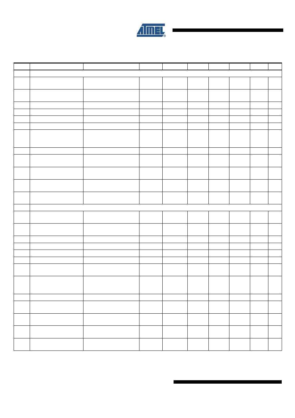
9.
Electrical Characteristics (Continued)
5V < V
S
< 27V, –40°C < T
j
< 150°C, unless otherwise specified. All values refer to GND pins
No.
Parameters
Test Conditions
Pin
Symbol
Min.
Typ.
Max.
Unit
Type*
*) Type means: A = 100% tested, B = 100% correlation tested, C = Characterized on samples, D = Design parameter