Thermal characteristics, Electrical characteristics – Rainbow Electronics ATA6630 User Manual
Page 23
23
9117C–AUTO–10/09
ATA6628/ATA6630 [Preliminary]
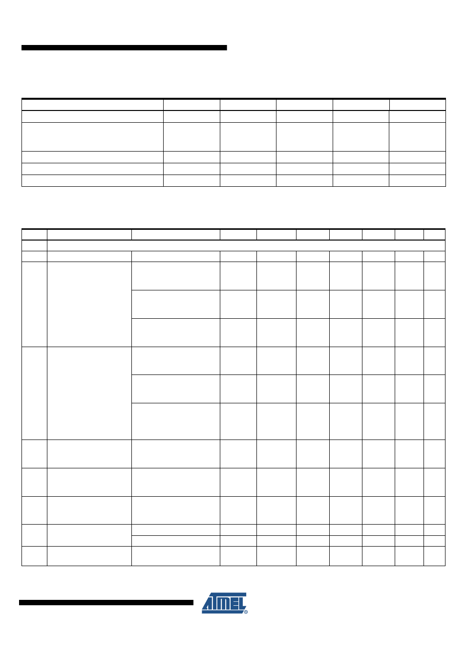
8.
Thermal Characteristics
Parameters
Symbol
Min.
Typ.
Max.
Unit
Thermal resistance junction to heat slug
R
thjc
10
K/W
Thermal resistance junction to ambient,
where heat slug is soldered to PCB
according to Jedec
R
thja
35
K/W
Thermal shutdown of VCC regulator
150
165
170
°C
Thermal shutdown of LIN output
150
165
170
°C
Thermal shutdown hysteresis
10
°C
9.
Electrical Characteristics
5V < V
S
< 27V, –40°C < T
j
< 150°C, unless otherwise specified. All values refer to GND pins
No.
Parameters
Test Conditions
Pin
Symbol
Min.
Typ.
Max.
Unit
Type*
1
VS Pin
1.1
Nominal DC voltage range
VS
V
S
5
27
V
A
1.2
Supply current in Sleep
Mode
Sleep Mode
V
LIN
> V
S
– 0.5V
V
S
< 14V (T
j
= 25°C)
VS
I
VSsleep
3
10
14
µA
A
Sleep Mode
V
LIN
> V
S
– 0.5V
V
S
< 14V (T
j
= 125°C)
VS
I
VSsleep
5
11
16
µA
A
Sleep Mode, V
LIN
= 0V
Bus shorted to GND
V
S
< 14V
VS
I
VSsleep_short
TBD
TBD
45
µA
A
1.3
Supply current in Silent
Mode
Bus recessive
V
S
< 14V (T
j
= 25°C)
Without load at VCC
VS
I
VSsi
30
40
50
µA
A
Bus recessive
V
S
< 14V (T
j
= 125°C)
Without load at VCC
VS
I
VSsi
30
40
50
µA
A
Silent Mode
V
S
< 14V
Bus shorted to GND
Without load at VCC
VS
I
VSsi_short
TBD
TBD
80
µA
A
1.4
Supply current in Normal
Mode
Bus recessive
V
S
< 14V
Without load at VCC
VS
I
VSrec
0.3
0.8
mA
A
1.5
Supply current in Normal
Mode
Bus recessive
V
S
< 14V
V
CC
load current 50 mA
VS
I
VSdom
50
53
mA
A
1.6
Supply current in Fail-safe
Mode
Bus recessive, RXD is low
V
S
< 14V
Without load at VCC
VS
I
VSfail
0.8
1.5
mA
A
1.7
VS undervoltage threshold
Switch to Unpowered Mode
VS
V
SthU
4
4.2
4.4
V
A
Switch to Fail-safe Mode
VS
V
SthF
4.3
4.5
4.9
V
A
1.8
VS undervoltage threshold
hysteresis
VS
V
Sth_hys
0.3
V
A
*) Type means: A = 100% tested, B = 100% correlation tested, C = Characterized on samples, D = Design parameter