Electrical characteristics (continued) – Rainbow Electronics ATA6630 User Manual
Page 26
26
9117C–AUTO–10/09
ATA6628/ATA6630 [Preliminary]
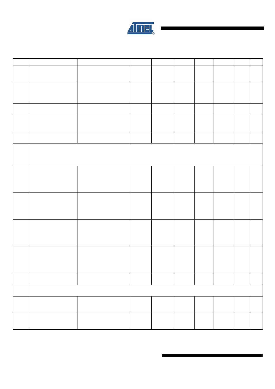
10.2
Time delay for mode
change from Fail-safe into
Normal Mode via EN pin
V
EN
= V
CC
EN
t
norm
5
15
20
µs
A
10.3
Time delay for mode
change from Normal
Mode to Sleep Mode via
EN pin
V
EN
= 0V
EN
t
sleep
2
7
12
µs
A
10.4
TXD dominant time-out
timer
V
TXD
= 0V
TXD
t
dom
27
55
70
ms
A
10.5
Time delay for mode
change from Silent Mode
into Normal Mode via EN
V
EN
= V
CC
EN
t
s_n
5
15
40
µs
A
10.6
Monitoring time for
wake-up over LIN bus
LIN
t
mon
6
10
15
ms
A
LIN Bus Driver AC Parameter with Different Bus Loads
Load 1 (small): 1 nF, 1 k
Ω
; Load 2 (large): 10 nF, 500
Ω
; R
RXD
= 5 k
Ω
; C
RXD
= 20 pF;
Load 3 (medium): 6.8 nF, 660
Ω
characterized on samples; 10.7 and 10.8 specifies the timing parameters for proper operation of
20 Kbit/s, 10.9 and 10.10 at 10.4 Kbit/s
10.7 Duty cycle 1
TH
Rec(max)
= 0.744
×
V
S
TH
Dom(max)
= 0.581
×
V
S
V
S
= 7.0V to 18V
t
Bit
= 50 µs
D1 = t
bus_rec(min)
/(2
×
t
Bit
)
LIN
D1
0.396
A
10.8 Duty cycle 2
TH
Rec(min)
= 0.422
×
V
S
TH
Dom(min)
= 0.284
×
V
S
V
S
= 7.6V to 18V
t
Bit
= 50 µs
D2 = t
bus_rec(max)
/(2
×
t
Bit
)
LIN
D2
0.581
A
10.9 Duty cycle 3
TH
Rec(max)
= 0.778
×
V
S
TH
Dom(max)
= 0.616
×
V
S
V
S
= 7.0V to 18V
t
Bit
= 96 µs
D3 = t
bus_rec(min)
/(2
×
t
Bit
)
LIN
D3
0.417
A
10.10 Duty cycle 4
TH
Rec(min)
= 0.389
×
V
S
TH
Dom(min)
= 0.251
×
V
S
V
S
= 7.6V to 18V
t
Bit
= 96 µs
D4 = t
bus_rec(max)
/(2
×
t
Bit
)
LIN
D4
0.590
A
10.11
Slope time falling and
rising edge at LIN
V
S
= 7.0V to 18V
LIN
t
SLOPE_fall
t
SLOPE_rise
3.5
22.5
µs
A
11
Receiver Electrical AC Parameters of the LIN Physical Layer
LIN Receiver, RXD Load Conditions (C
RXD
): 20 pF
11.1
Propagation delay of
receiver (
V
S
= 7.0V to 18V
t
rx_pd
= max(t
rx_pdr
, t
rx_pdf
)
RXD
t
rx_pd
6
µs
A
11.2
Symmetry of receiver
propagation delay rising
edge minus falling edge
V
S
= 7.0V to 18V
t
rx_sym
= t
rx_pdr
– t
rx_pdf
RXD
t
rx_sym
–2
+2
µs
A
9.
Electrical Characteristics (Continued)
5V < V
S
< 27V, –40°C < T
j
< 150°C, unless otherwise specified. All values refer to GND pins
No.
Parameters
Test Conditions
Pin
Symbol
Min.
Typ.
Max.
Unit
Type*
*) Type means: A = 100% tested, B = 100% correlation tested, C = Characterized on samples, D = Design parameter